This is a straight continuation from IDD.
Binary Codes
Binary codes can be used to represent information. The most common formats are pure binary (for numbers), which is weighted and ASCII (for characters) which is unweighted.
What is weighted?
It is positional notation, e.g., 3456 = 3 × 10⁴ + 4 × 10² + 5 × 101 + 6 × 100. For binary, this could be: 0111 = 0 × 23 + 1 × 22 + 1 × 21 + 1 × 20. 0 + 4 + 2 + 1 = 7.
To distinguish pure binary, you could say it was the 8421 code (from the column weightings).
The pure binary sequence has occurances where multiple digits need to change (e.g., 0111 -> 1000). The multiple digits may change at different rates, so erroneus intermediate states may be generated - causing hazards.
Another code is grey code that is used to minimise hazards. The grey code is reflected and unweighted.
Grey Code
Everything but the left-hand column is reflected by the mid-point. The left-most column is reflected instead. You repeat moving down each column.
Binary Coded Decimal (BCD) codes
BCD codes can represent the decimal numbers 0-9. Different codes could be:
- 8421 BCD
- 7421 BCD
- 5421 BCD
- 5211 BCD
- 84 BCD
- Excess-3 BCD
- Grey BCD
In most cases, the names come from the weightings. Excess-3 is where you add 3 to every pure-binary number (8421) to get the Excess-3 BCD.
Error Detection Codes
See Introduction to Computer Systems for more information and parity, Hamming detection and Hamming distance.
Minimum distance is the number of bits that need to be changed to make another valid word.
An SN74LS180 is a device that is a parity generator/checker.
Sequential Circuits
In addition to combinatorial circuits, which we have seen so far, we also have sequential circuits.
Combinatorial circuits are ones whose outputs depend on the current input state. When inputs change, the outputs do not depend on the previous inputs.
Sequential circuits are similar, but they do also rely on previous input states. It can be inferred that they have memory.
The outputs can be taken directly from the memory elements also.
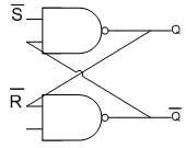
Memory Elements
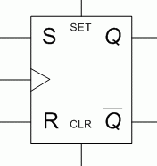
These are called bi-stables, or flip-flops. They are capable of storing 1 bit of data as long as they are powered. Generally, there are two outputs, Q and which give opposite outputs. There is also typically a CLK (clock) input and reset lines (which are independant of the clock and are active-low, meaning they float high, and can be left hanging).
The type of flip-flop determines the state to which they switch and the inputs give them their name: SR, D, T and JK.
Clock
A step-down transformer can be used with a Zener diode and a Schmitt trigger inverter to generate a clock based on mains voltage (50 Hz). Mains voltage is regulated so that a clock based on it will never be more than a minute out.
Crystals can also be used to create a stable frequency, but long-term drift does occur.
Types of Sequential Circuit
Synchronous
The same clock signal is applied to each flip-flop, and changes in state occur when the clock changes state from one level to another.
Asynchronous
The behaviour of an asynchronous circuit depends on the order in which the inputs change. Sometimes, there is an input labelled clock, that provides some level of synchronisation, but it is normally only applied to one flip-flop. In addition to this style of asynchronous circuit, you also get gate-level asynchronous circuits, which are combinatorial circuits with feedback.
Gate-level Asynchronous
A gate level asynchronous circuit looks like this:
And this can also be redrawn to make a flip-flop.
Flip-flop characteristic tables are like truth-tables, but for sequential circuits. They show the states of inputs and outputs after the clock arrives.
D-type
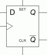
| D | Q(t+1) |
| 0 | 0 |
| 1 | 1 |
The value of D is transferred to Q after the clock arrives.
T-type
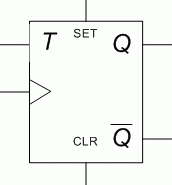
| T | Q(t+1) |
| 0 | Q(t) |
| 1 |
The value of T determines whether or not Q should change state (toggle).
JK-type
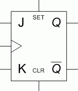
| J | K | Q(t+1) | Meaning |
| 0 | 0 | Q(t) | no change |
| 0 | 1 | 0 | reset |
| 1 | 0 | 1 | set |
| 1 | 1 | toggle |
The JK is a general purpose flip-flop.
SR-type
| S | R | Q(t+1) | Meaning |
| 0 | 0 | Q(t) | no change |
| 0 | 1 | 0 | reset |
| 1 | 0 | 1 | set |
| 1 | 1 | don't use |
From the JK-type, you can make other types of gate. For example, by attaching a line to J and K, you have a T-type, or by attaching a line to J and the inverted linke to K, you have a D type gate, and the SR is similar to JK anyway. You can also make a JK-type from the other types, but it's more complicated.
Sequential Circuit Analysis
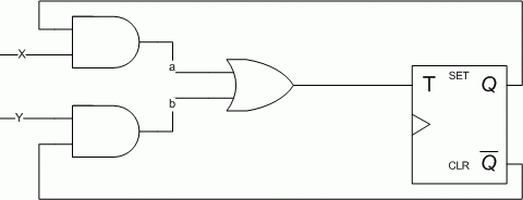
| X | Y | Q(t) | a | b | T | Q(t+1) |
| 0 | 0 | 0 | 0 | 0 | 0 | 0 |
| 0 | 0 | 1 | 0 | 0 | 0 | 1 |
| 0 | 1 | 0 | 0 | 1 | 1 | 1 |
| 0 | 1 | 1 | 0 | 0 | 0 | 1 |
| 1 | 0 | 0 | 0 | 0 | 0 | 0 |
| 1 | 0 | 1 | 1 | 0 | 1 | 0 |
| 1 | 1 | 0 | 0 | 1 | 1 | 1 |
| 1 | 1 | 1 | 1 | 0 | 1 | 0 |
Note: Y is equivalent to J and X to K.
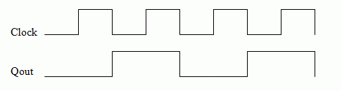
Frequency Division by 2
Shift Registers and Counters
Shifting and Dividing
When D-type flip-flops are connected in parallel, inputs are passed from one flip-flop to the other, providing a shifting operation. The shift loses the least significant bit, causing the divide to be rounded down. A 0 must be shifted onto the word for it to work. If you left-shift, you can multiply by 2, but this time, the most significant bit is lost.
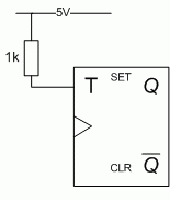
A T-type flip-flop has only half the period of the input signal, therefore can be used for dividing by 2. Connected in series will lead to dividing by 2, 4, 8, etc...
Universal shift registers (SN74AS194) can be used to do shift left or right, so you can multiple of divide. They can also be parallel loaded.
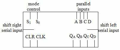
The modes can be controlled as follows:
| S1 | S0 | Action |
| 0 | 0 | Inhibit clock |
| 0 | 1 | Shift right |
| 1 | 0 | Shift left |
| 1 | 1 | Parallel load |
Parallel Loading
Asynchronous Counter
Because you can use T-types to divide, if you make them asynchronous and put them in serial, you can create a counter. By attaching the T-type to 1, and then using Q to power the clock for all flip-flops after the first one, you can inspect Q for each flip-flop to get a binary word representing the current value in the word.
Then, by combining for the first flip-flop with Q for each subsequent flip-flop into a NAND, and then into the CLR circuit, you can reset the counter to prevent overflow.
Sequential Circuit Design
Mealy Machine
This is sometimes referred to as a Class A machine.
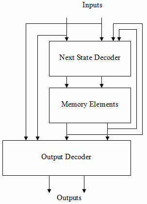
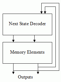
The outputs are a function of the current state (according to the memory elements) and the inputs, according to the output decoder. The next state decoder determines the next-state to be held in the memory elements. It is assumed there is also a clock for the memory elements.
Moore Machine
This is sometimes referred to as a Class B machine.
A Mealy machine is like a class A machine, but the output is only a function of the current state, and not the outside world.
Class C Machine
A Class C machine is like a Class B machine, but with no output decoder.
Class D Machine
A Class D machine has no outside world inputs, i.e., it is a pure signal generator.
State Diagram
A state diagram is a pictorial representation of the state table.
| Present State | Inputs | Next State | Outputs | ||
| A | B | x | A | B | y |
| 0 | 0 | 0 | 0 | 0 | 0 |
| 0 | 0 | 1 | 0 | 1 | 0 |
| 0 | 1 | 0 | 0 | 0 | 1 |
| 0 | 1 | 1 | 1 | 1 | 0 |
| 1 | 0 | 0 | 0 | 0 | 1 |
| 1 | 0 | 1 | 1 | 0 | 0 |
| 1 | 1 | 0 | 0 | 0 | 1 |
| 1 | 1 | 1 | 1 | 0 | 0 |
For the above state table, the state diagram would look like:
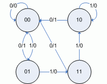
The circle shows the current state and the arrow show what transition occurs with that x/y value pair. Note, the values are the values after the transition, when the circuit has become stable.
Excitation Tables
When designing a sequential circuit, it is necessary to know what inputs are needed to trigger the desired transition (as given in the design). An excitation gives this information, and is kind of a reverse characteristic table.
D-type
| Q(t) | Q(t + 1) | D(t) |
| 0 | 0 | 0 |
| 0 | 1 | 1 |
| 1 | 0 | 0 |
| 1 | 1 | 1 |
T-type
| Q(t) | Q(t + 1) | T(t) |
| 0 | 0 | 0 |
| 0 | 1 | 1 |
| 1 | 0 | 1 |
| 1 | 1 | 0 |
SR-type
| Q(t) | Q(t + 1) | S(t) | R(t) |
| 0 | 0 | 0 | X |
| 0 | 1 | 1 | 0 |
| 1 | 0 | 0 | 1 |
| 1 | 1 | X | 0 |
JK-type
| Q(t) | Q(t + 1) | J(t) | K(t) |
| 0 | 0 | 0 | X |
| 0 | 1 | 1 | X |
| 1 | 0 | X | 1 |
| 1 | 1 | X | 0 |
From the excitation tables from the individual flip-flops, it is possible to create an excitation table for a sequential circuit. The table is broken up into 3 sections: Current state; Next state; and Flip-Flop Inputs. The Current State column lists the state before the clock edge, the Next State lists the state required after the clock edge, and the Flip-Flop Inputs list the inputs each input requires to get that desired Next State.
Flip-Flop Selection
Although the choice of flip-flops is often out of your control, if you do have a choice over which flip-flops you could use, some are better suited to tasks then others.
- D-type flip-flops are best for shifting operations (e.g., shift registers).
- T-type flip-flops are best for complemention operations (e.g., binary counters)
- JK-type flip-flops are best for general applications (they are the most versatile, and it is the easiest to make the other types out of)
- SR-type flip-flops are safe to use also, as long as the circuit is designed properly, so the 1,1 condition never occurs across the inputs.
The basic steps to sequential circuit design are as follows:
- Create the state diagram from the written specification
- Minimise the number of values (state reduction)
- Assign binary values to the states (state assignment)
- Select the flip-flops to be used
- Create the excitation table for the circuit
- Minimise each next state decoder output
- Minimise each output from the output decoder
- Analyse the design and check it meets the specification
There are additional stages to consider in sequential circuit design which can be found in the online DAD notes.
Asynchronous Analysis of Flip-Flops
Modern flip-flops change on a clock edge. Early flip-flops changed on the pulse itself, which led to difficulties when combining flip-flops into counters and registers.
Switch Debounce
When a mechanical switch is thrown, the contact vibrates a few times before settling in a state. The amount of vibration is unpredictable, but leads to a sequence of pulses from 0 to 1 rather than a simple transition. If this switch is clocking a signal generator, it will not change state on one application of the state, but clock through a variety of states, the number being unpredictable.
A debounce circuit - based on the flip-flop - is required to correct this problem.
The mechanical switch used in this circuit must be a make-before-break circuit - it must break contact before it makes the next contact.
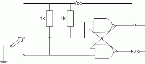
flip-flop
In the characteristic table for the SR flip-flop, we can see that we should never set SR to 11. Similarly, we should never set a flip-flop to 00. Doing this causes an unstable state that causes Q and to oscillate between 00 and 11 forever due to the feedback. In reality, however, this does not really happen, as one gate will be faster than the other, and it'll settle unpredictably on 01 or 10.
Although the inputs are inverted to form an SR flip-flop from a flip-flop, the same problem remains.
Asynchronous Analysis
If we consider the flip-flop where a and b are the inputs and x and y are the feedbacks from the outputs, we can draw two transition tables:
A =
| ab\xy | 00 | 01 | 11 | 10 |
| 00 | 1 | 1 | 1 | 1 |
| 01 | 1 | 1 | 0 | 0 |
| 11 | 1 | 1 | 0 | 0 |
| 10 | 1 | 1 | 1 | 1 |
B =
| ab\xy | 00 | 01 | 11 | 10 |
| 00 | 1 | 1 | 1 | 1 |
| 01 | 1 | 1 | 1 | 1 |
| 11 | 1 | 0 | 0 | 1 |
| 10 | 1 | 0 | 0 | 1 |
We can then combine the two:
| ab\xy | 00 | 01 | 11 | 10 |
| 00 | 11 | 11 | 11 | 11 |
| 01 | 11 | 11 | 01 | 01 |
| 11 | 11 | 10 | 00 | 01 |
| 10 | 11 | 10 | 10 | 11 |
The ringed terms indicate stable states.
Races in Asynchronous Circuits
Mano p347-348
A race condition is said to exist in an asynchronous sequential circuit when two or more binary state variables change state in a response to a change in input variable. When unequal delays are encountered, a race condition may cause the state variables to change in an unpredictable manner.
If the final state of the circuit does not depend on the order in which the state variables change, the race is called a non-critical race. If it is possible to end up in two or more stable states depending on the order in which the state variables change, this is called a critical race.
Analysis of a transition table can show race conditions, but it does assume 0 gate delay, which is not true. The transition table can not predict the behaviour of a circuit where a precisely timed enable line ensure correct logical behaviour.
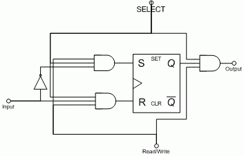
Enabling Flip-Flops
If you use a NAND inverter into a flip-flop, and then use the spare input, you can make an enabling line. When the enable line is low, S and R can take any input and Q and will not change. When the enable line is high, it will behave like a normal SR flip-flop. This enabling mechanism is sometimes called a level-sensitive clock.
If you invert S in the above circuit and connect it to R, you will get an enabled D-type flip-flop, which is a well-behaved circuit called a latch - which is still widely used.
Transition table analysis
can be found for common
flip-flop types on the
lecture slides.
Hazards
A logical analysis of an asynchronous circuit can be achieved by breaking the feedback links and forming a Karnaugh map. As a Karnaugh map, static hazards can be determined.
Essential hazards occur when an input changes and this is not detected by all the excitation circuits before the state variables are sent back to the excitation circuits.
Modern Flip-Flop Clocking Mechanisms
Early flip-flops had enabling/disabling clocks - these were called level-sensitive. Although early SR and D-types were well behaved, the T and JK types required the enabling clock pules widths to be precisely set for each flip-flop.
The basic enabling clock pulse made D-type flip-flops connected in a shift register difficult to be controlled. The pulse duration had to be shorter than the input-ouput delay of the flip-flop.
Modern flip-flops are synchronised on the edges (transitions) of the clock, not the pulses (levels). There are three basic mechanisms for implementing this - edge-triggered, master-slave and master-slave with data lockout - and they are either positive edge clocking (on the rising edge) or negative edge clocking (on the falling edge). Once the clock has passed the threshold, the inputs are locked out and is unresponsive to changes on the input. There are finite times when the inputs must not change. These are:
- Setup time (tsu) is the time for input data to settle in before the triggering edge of the clock occurs. Typical value is around 20 ns, but in reality this is shorter.
- Hold time (th) is the time required for the input data to remain stable after the triggering edge of the clock occurs. Typical value is around 5 ns, but in reality this is shorter.
In a manufacturers data book, minimum values are specified, which is the shortest intervals for which correct operation is guaranteed.
The propogation delay of a flip-flop is defined as the time between the clock reaching the clocking threshold (the transition point) and the outputs responding to the flip-flop inputs as they were, immediately before the clock acheived the threshold.
Master-Slave Flip-Flops
A master-slave flip-flop consists of a master flip-flop of the basic types (D, T, SR or JK) and a slave flip-flop (an SR type) with an inverted clock.
The setup time is determined by the pulse width and the hold time is 0. On the rising edge two things happen - the master is isolated from the slave and the inputs are read. On the downward edge, the flip-flop inputs stop being read and the master is connected to the slave.
The clocking edge can be positive or negative according to the device.
The states of the input should not change while the clock is high, otherwise the master is set or reset and can not be changed again and the output of the slave will change accordingly. This is a problem with synchronous sequential circuits with asynchronous inputs and the input changes when the clock is high. A data-lockout variation of the master-slave flip-flop is used that allows the device to load the next stage information into the flip-flop on the preceeding edge waveform.
In a data-lockout flip-flop, there is a setup and hold time during which the inputs must not change. After the hold time has expired, the inputs may change without creating erroneus results. After the clocking edge (and propogation delay), Q will change accordingly. The hold time after the clocking edge is 0.
Synchronising Asynchronous Circuits
Synchronous circuits which are controlled by asynchronous inputs may cause flip-flop inputs to change during setup and hold periods - such changes may cause an inappropriate jump in sequence. It is important to synchronise the asynchronous inputs so they do not occur during setup and hold times - this is acheived by latching (with a latch) or registering (with a register) the inputs.
When the input changes during the flip-flops setup time, metastability can become a problem. The output is unstable for some time before it settles to a stable state and the output level can be halfway between 0 and 1 and be recognised inconsistently as either 0 or 1. The length of time the output is metastable is unpredictable.
Synchronous Circuit Timing Constraints
A flip-flop is limited in speed by the switching times of the transistors that make up the flip-flop. The speed of the clock is determined by such factors as: the propogation delay of the flip-flop, the propogation delay of the next-state decoder and the setup time of the flip-flop.
Maximum Flip-Flop Clocking Frequency
This is the highest rate a bistable circuit can be driven whilst still maintaining stable logic transitions and states. Minimum values are 20-25 MHz and typical values are more like 25-33 MHz.
Minimum Flip-Flop Pulse Duration
The time interval between specified reference points (about 1.3 V on each edge) on the leading and trailing edge of the pulse waveform. Minimum values are 20-25 ns.
Races in Synchronous Circuits
A synchronous circuit behaves correctly if the flip-flop inputs do not change during their hold time. Where flip-flops are coupled together directly with a common clock, the output changes after the propogation delay of the clock has elapsed. That delay must be longer than the hold time of the next device so it does not see a change during it's hold time. However, if flip-flops from different families are connected, this could cause a problem. This is why 0 hold time is important.
Clock Skew
In a synchronous sequential circuit, all flip-flops are supposed to be clocked at the exact same time. If this does not happen, it causes clock skew. Clock skew can be caused by:
- unequal gate delays in clock buffers
- unequal wire length
- unequal clock threshold voltage
A small amount of clock skew is tolerable, however. To determine the clock skew tolerance, the minimum flip-flop propogation delay needs to be known, but this is not always given in manufacturer's data sheets. The guaranteed minimum setup time (the actual will probably be less) also needs to be known. For master-slave devices with data lockout, the effective allowable clock skew is the minimum propagation delay minus the setup time plus the clock pulse width. Thus, the designer can set the maximum allowable clock skew needed by changing the pulse width.
Computer Memory
There are different types of computer memory:
- Magnetic Disk - non-volatile data not immediately needed, often called backing store or secondary memory.
- Integrated Circuit Random Access Memory - volatile data immediately needed, this is main or primary memory. Main memory is often supplemented by fast register-based that stores some of the items that have been recently stored in or accessed from main memory. This is called cache memory and exists to speed up memory access.
- ROM - non-volatile, usually used for containing bootup instructions. ROMs also store micro-instructions that define the instruction set of a central processor. Some CPUs allow micro-instructions to be changed, thus redefining the instruction set. In some cases, the instruction set could be changed to make particular programs and languages run more efficiently, e.g., PERQ.
RAM comes in two main forms: SRAM (Static), based on flip-flops and DRAM (dynamic), based on storage of charge. DRAM allows for approximately 4 times greater chip density, but in reading back data in DRAM, the charge is destroyed and must be written back, requiring greater circuit complexity. DRAM is slower than SRAM, but uses less power.
See ICS/CAR for
information about
organisation of
memory
To connect to RAM, you need to select an address (mar/memory address register), a read/write control and data in/out lines (mbr/memory buffer register).
SRAM
An SRAM cell looks like:
A bank of cells forms RAM. In an 8 bit word, 8 cells are in parallel, and a decoder selects which line to read.
Memory Address Decoding
Memory chips include a decoder that converts the address into the corresponding word in memory to be accessed. An AND gate is used to perform this decoding and there is one AND gate driving the enabling control line. A million word memory requires at least a million AND gate, with each AND gate having 20 inputs (as in a parallel decoder).
So as the address requirement becomes large, the number of inputs to each AND gate becomes less tractable to provide, so alternative structures such as the balanced decoder or tree decoder are adopted.
A parallel decoder is just a normal decoder as looked at before, however a tree decoder works in multiple stages, with one bit being added at each stage, meaning only 2-input AND gates are needed.
A balanced decoder is similar but backwards. Two inputs are mixed together, and then the outputs from those are mixed together until the final mixing stage at the end.
| Decoder Type | No. of Address Lines | No. of Output Lines | No. of AND gates | No. of AND gate inputs | Levels of delay |
| Parallel | 4 | 16 | 16 | 64 | 1 |
| Tree | 4 | 16 | 28 | 56 | 3 |
| Balanced | 4 | 16 | 24 | 48 | 2 |
The parallel decoder is probably fastest, but the balanced decoder is probably most practical.
The output/input lines are often passed through bus drivers/receivers, so that the same pin on the package can be used for both input and output and can be connected directly to a bus. The basic memory cell is a latch that is enabled by the select line going high. Prior to the falling edge there is a setup time criteria to be met and after the falling edge there is a hold time criteria to be met.
Since the input data and write-enable signal is applied to each word, it is important for the address to be stable before the memory enable occurs, otherwise the data could be placed in the wrong word.
Memory access time is the time it takes to obtain stable output data after the word has been selected - this is what is meant by 20 ns RAM. CMOS RAM has access times in the order of 15 ns, whilst TTL/CMOS has access time of around 3 ns.
Static RAM is often used as cache memory in DRAM-based high performance computers. This enhances their performance by storing previously accessed or written data, or storing the data in contiguous blocks of memory.
See ICS for more
information on error
correction
Both SRAM and DRAM can suffer from occasional errors in the stored data due to many factors, such as cosmic rays. Hamming codes can be used to aid detection of words.
DRAM
A 64 k 1-bit DRAM is physically constructed as a 256 × 256 array of bits. 16 bits of address are needed to address the 1-bit word. The address is presented as 2 8-bit words in sequence requiring a row address strobe (RAS) and a column address strobe (CAS). To refresh, the RAS line is made high, the address is stored and the whole row is stored in a 256-bit latch. Then RAS goes low and the row is written back from the latch.
In the read cycle, a row is specified and stored in the 256-bit latch. A column is then read and stored in the column address register. A multiplexer is then used to select 1 bit from the row latch which is made available at the output. The row address strobe goes low and the row is written back.
In the write cycle, the row is addressed and stored in the 256-bit latch. WE (Write Enable) is asserted and then CAS is asserted. The bit on the input line is read into the 256 bit latch (using a demultiplexer) using the column address register and the latch is written back into the array when the row address strobe falls to zero.
It is possible to read/write part or all of a row before the writing back process occurs.
Binary Arithmetic
The decimal number system is a positional number system, with numbers in different columns weighted at base 10. The binary number system is identical, but with base 2.
In digital systems, registers are finite in size and limit the number of digits. If the computation generates a number that is too big for the register, an overflow will occur. In a computer system, this is often caught as an interrupt. If you wanted to add two n-bit positive numbers, you would need an (n + 1)-bit register to hold the result.
Binary subtraction happens in much the same way as decimal, so a subtraction circuit must examine signs and magnitude and decide what operation to perform and then figure out the sign of the result. This is complex, so two's complement is used.
The benefit of this is that two positive or negative integers can be added together to produce the correct result. To convert a binary number into two's complement involves forming the one's complement (flipping all the bits) and adding 1. Therefore, a two's complement number with 0 for the msb indicates a positive number, whereas one with the msb set to 1 indicates a negative number, which must be converted back to a normallised number for humans to digest.
If subtraction uses two's complement, an addition circuit can be used for both addition and subtraction. If two n-bit positive numbers are to be added, then the result requires (n + 1) bits to store, so giving that the msb signifies the sign of the number, two n-bit numbers engaged in adding or subtracting requires (n + 2) bits for their storage and result.
Binary multiplication is similar to decimal multiplication:
- Multiply (AND) single digits
- Shift (by the position of the multiplier)
- Add to the accumulator.
If we multiple a negative (two's complement) number by a normal one, we must do two's complement on the answer to get the correct answer. If two n-bit positive numbers are being multiplied, then we might need up to 2n bits to store the result. In the case of a negative number, this becomes (2n + 1).
Binary division is a trial and error process based on long division in decimals. At each step a trial division is made by subtracting the divisor. If the result is positive, the divisor goes into the dividend, so the appropriate quotient digit becomes 1. If the result is negative, the quotient digit becomes 0 and the divisor is added back.
Handling negative numbers is often handled by converting them to unsigned integers and then applying rules to handle the signs (XOR).
Division using two's complement is possible, but is more complex than this method.
The form of numbers looked at so far are called fixed point numbers. Our digits are weighted by a fixed position. As such, we can continue down the weighting (2-1, 2-2, etc). This also works for two's complement. The accuracy of such a number is limited by the amount of bits you have, so some rounding may be required.
IEEE floats were
covered in ICS.
We can also use floating point numbers, which are defined by an IEEE standard. There is a 1 bit sign (S), an 8-bit exponent (E) and a 23-bit fractional mantissa. A floating point number is computed from this representation by: X = (-1)S × 2E - 127 × (1 + F). There are also special cases to allow representations.
Two's complement also creates a problem with zero. We are only allowed one representation for 0, but there is an extra negative number (-2n - 1 that has no positive counterpart (although it is 1000, it does not behave like 0). Care must be taken to ensure this number is not used.
Two's complement numbers can be used inside the PC without constantly converting to another form (although it must be converted for outside the computer use), however left and right shifting for multiplication and division does not work with two's complement,.
Adding and Subtracting in Hardware
Normally if A-B, the magnitude of B is converted to its two's complement and added to A. If the msb of the result is 1 then the result must be two's complemented to obtain the magnitude of the negative number.
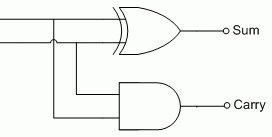
We can create a half-adder by truth table analysis:
| A | B | Sum | Carry |
| 0 | 0 | 0 | 0 |
| 0 | 1 | 1 | 0 |
| 1 | 0 | 1 | 0 |
| 1 | 1 | 0 | 1 |
So, Sum = A XOR B and Carry = AB.
A full adder needs to consider the previous carry bit when adding, so this gives us a new truth table:
| A | B | Ci-1 | Sum | Carry |
| 0 | 0 | 0 | 0 | 0 |
| 0 | 0 | 1 | 1 | 0 |
| 0 | 1 | 0 | 1 | 0 |
| 0 | 1 | 1 | 0 | 1 |
| 1 | 0 | 0 | 1 | 0 |
| 1 | 0 | 1 | 0 | 1 |
| 1 | 1 | 0 | 0 | 1 |
| 1 | 1 | 1 | 1 | 1 |
We can conventionally minimise this, but another solution is to write it out in the canonical form and use boolean algebra. Using this, Sum = A XOR B XOR Ci-1 and carry = AB + (A XOR B)Ci-1. Therefore, we can implement a full adder using two half-adders (XOR's can only have 2 inputs, so we need to chain them).
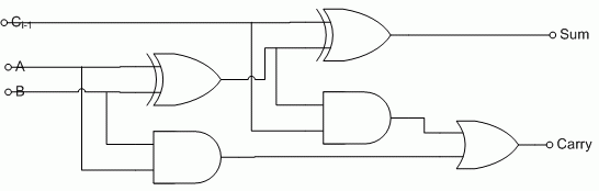
Although this is the standard textbook design of a full adder, due to constaints with the speed of the carry, they aren't really implemented like this. A full-adder is deduced using map factoring (Karnaugh maps and some intuition), which is likely to be less hazardous due to lots of looping.
A 4-bit binary adder uses parallel binary adding, with the adders connected in serial. However, the correct addition of a bit depends on the states of the carry bits before it - leading to a "ripple effect" of carry bits being computed and the correct answer propogating through. This ripple effect determines the operational speed.
We should use look-ahead carry to increase the speed of our adder.
The look-ahead carry provides parallel generation of each carry bit at the expense of additional gates. The sum function for the full-adder remains the same, but the carry function is reconsidered.
Two carry bits are needed, a generate and propagate:
- G = AB
- P = A XOR B
So the carry function becomes: C = G + PCi-1 and the sum function becomes: S = P XOR Ci-1. Both of these terms can be generated using half-adders.
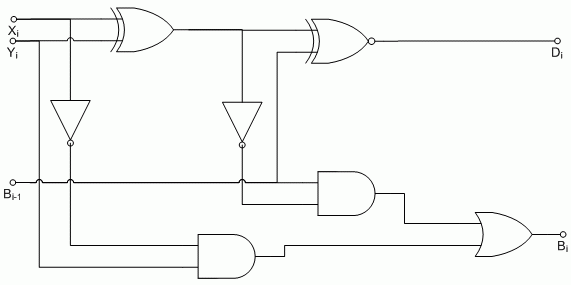
Subtraction uses two's complement. By using XOR gates and a mode line connected to the gates and Cin you can invert the inputs and then add 1, giving you the numbers in 2's complement. By setting the mode line to 0 normal addition can still occur on the same gate.
Truth table analysis would give us an expression for the subtractor which can then be used to construct a circuit.
Comparators and ALUs
A comparator compares two binary words for equality. Most also provide arithmetic relationships between them - i.e., outputs indicating greater than or less than. Generally the arithmetic output assumes the words only represent a magnitude.
ALUs are covered
in CAR and ICS
Arithmetic Logic Units provide arithmetic and logic operations on a pair of words.
XORs into a NOR gate or XNORs into an AND gate provide an equality test.
If you realise an XNOR in 5 gates, you can also extract greater than and less than from the internal nodes, as well as equality from its output.
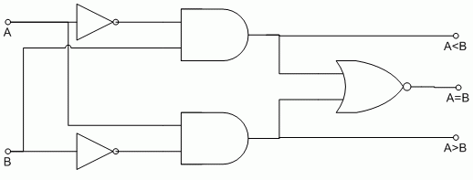
Comparators (SN74LS85) can be chained, so they normally have 3 additional inputs: AGTBIN, ALTBIN, AEQB, which are taken into account when a comparison is done.
ALUs come in different sorts, and provide different operations on the inputs depending on what is needed of them. For example, the SN74LS181 provides a 4 bit function selector and a 1-bit mode selector that allows it to choose between logic or arithmetic mode.
ALUs can be cascaded, so they often have additional inputs such as CIN (carry in), P and G (carry propagate and generate) and COUT (carry out).
Multiplying and Dividing Integers
One way of doing integer multiplication is repeated addition, e.g., 3 × 4 = 4 + 4 + 4. You should select the smaller number to minimise the number of adds, and this is implemented using a sequential circuit. Another way of implementing this is using shifting and adding. m bits numbers require m shift-and-add operations. This is also a sequential circuit. The final implementation method is by designing a combinatorial circuit that accomodates all possible combinations of inputs.
If the maximum bit size for unsigned integers is n bits, then 2n bits are required to store the results. If negative numbers are to be accomodated, then 2n+1 bits are needed.
To do repeated addition, feedback from an adder is used for one word and then the other word is the other input from an adder. A down-counter connected to inhibit the clock when it reaches 0 is used to control the number of additions.
Shift-and-add is similar, but a shift register is used to control the adding process, and the second word is also attached to a shift register. If negative numbers are to be handled, then the registers and adder must be n+1 bits wide.
Standard combinatorial logic can be used to create a combinatorial multiplier. Combinatorial multipliers can also be chained together. For example, you can create a 4 × 4 multiplier with 4 2 × 2 multipliers like so:
A × B = (ALSB × BLSB) + 2((ALSB × BMSB) + AMSB × BLSB)) + 4(AMSB × BMSB)
Array based multipliers, which is based on the AND gate can also be used. Here, half-adders and full-adders are combined to cascade the output for multiple-byte addition. Array-based multipliers can be combined in a building block for VLSI replication.
For division, negative numbers are normally converted to unsigned, and then the final sign is figured out by rule. One method of division is to keep subtracting the divisor from the dividend until the result of the subtraction is negative - the number of repetitions less 1 is the quotient. To the negative result, you then add back the divisor to obtain the remainder.
Given that a fast multiplier may already exist, it is possible to consider an approach based on it. dividend = (divisor × quotient) + remainder. The quotient is set to 0, and then increment, multiply the quotient and divisor, and if the result is greater than the divided, stop and decrement the quotient for the correct answer.
You can also use restoring division, based on shift and subtract, except when the subtraction results in a negative number, the divisor must be added back.
Non-restoring division is similar, except that when the subtraction results in a negative number, the divisor is shifted and added. This results in n additions, compared with an average of 1.5n additions for the restoring divisor. This is a fast, sequential process.
Combinatorial dividers exist which offer parallel division, but there are not covered.
Sequential Programmable Devices
Sequential programming devices are extensions to the PLDs we've already covered in IDD.
A simple way of deriving a sequential circuit using a PLD is to feed the outputs of a combinatorials PLD into D-type registers. Many sequential PLDs already have D-type registers built in, with the input lines of the PLD taking feedback from the output of the flip-flops.
The registers have a common clock and clock on a rising edge, therefore we can create synchronous only circuits. They have a setup time and an (effectively) zero hold time (because of the AND-OR propogation delays). There are also preset and clear lines which are independent of the clock.
On power-up, the registered outputs are usually set low, and the outputs are usually tri-state.
An XOR PAL (programmable array logic) can be used to change the type of flip flop in the register. J and K can be simulated by using two AND gates, one with K and Q and the other with J and into an OR gate (replicating a T-type) with Q and T going into the XOR gate leading to the flip-flop.
Although the registered PAL can be used to provide a sequential circuit, the D-type is not ideal for counters, however, with the XOR gate interposed between the OR stage and the D input can provide resetting, holding and toggling. You could consider a binary counter as "the current value, plus one". For the lsb, 1 is added (and there is no carry), but for all other bits, there may be a carry from a less significant bit. Once the addition has taken place by the PLD, the next value of the counter is available at the D inputs which is then transferred to the clocking outputs at the next clocking cycle.
Analogue Circuits
Analogue linear circuits are the opposite to digital circuits in that a range of voltages can exist in a circuit. With linear circuits, relationships are proportional (as in V = IR, V against I is linear with the constant of proportionality is R).
Electricity
Electricity is an energy supply that is convenient to produce, distribute and use. Emf (Electromotive force) causes electric charge to flow. Charge (Q) is the measure of the surplus or deficit of of electrons and is measured in Coulombs. The smallest amount of charge possible is the charge on an electron (1.6 × 10⁻¹⁹ C) which is denoted with the symbol e.
Electric current (I) is the rate at which charge flows (I = dQ/dt). Current can only flow in closed paths, so we speak of electric circuits. A useful electric circuit consists of at least one device that produces a desired effect and an energy source that can maintain a current throughout the circuit.
The fundamental quantities to be found in electric circuit analysis are voltage (V) and current (I). These two are related, since the voltage across a device drives a current through it, or a current through a device generates a current across it.
Potential difference is the work (measured in Joules (J)) required to move a unit of positive charge (1 C) between two points - E = QV. It is a measure of the force which tends to move charge from one point to another. Potential difference relative is ground (0 V) is often just called potential. Emf is the potential difference from a voltage source, such as a battery.
Ohm's Law
In conductors, charge can move easily. In insulators, charges can't move easily.
Ohm's Law states that the potential difference across a conductor is proportional to the current through it. The constant of proportionality is called resistance (R) and is measured in Ohms (Ω). This gives us V = IR.
Resistors are used for voltage to current conversion, or vice-versa. They are rated for their ability to dissipate power. The inverse of resistance is called conductance (G) and is measured in Siemens (S). This gives us V = I/G.
Power
We know that E = QV, however if we measure change across time, then V is a constant and dE/dt = dQ/dt V. We know that power is the change in energy over time and current is the change in charge over time, so we can derive that P = IV. This is measured in Watts (W) or Joules per second (Js-1).
Ideal Sources
As we mentioned earlier, some kind of power source is required for the circuit to be useful. In circuit analysis, it is often convenient to think about idealised energy sources.
An ideal voltage source is independant of the current passing through it and an ideal current source is independant of the voltage across it.
Real sources are modelled as ideal sources in combination with a resistance, called the internal resistance.
Kirchoff's Law
Kirchoff's First (Current) Law
The sum of the current entering any node is equal to 0 (Σi = 0).
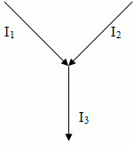
According to Kirchoff's Current Law, I1 + I2 = I3
Kirchoff's Second (Voltage) Law
The sum of all potential differences around any closed path is 0. (Σv = 0).
e.g., if you have a voltage source (V1) and two devices in the circuit (V2 and V3) - V1 = V2 + V3
Capacitance
If we move Q Coulombs of charge between 2 uncharged conductors, the voltage difference, V, between the two conductors is proportional to Q such that Q = VC, where the constant of proportionality is called the capacitance of the conductor arrangement. It depends on factors such as the shape and size of the conductors and the material or dielectric between them. Capacitance has units in Farads (F), but typical circuit values are in the microfarad (µF) range or smaller.
From Ohm's Law, we can derive that I = C dV/dt.
Inductance
If, in a coiled conductor, current is changing with time, it generates a magnetic field which is changing with time. This induces a voltage across the coil itself with tends to oppose the current. The voltage is proportional to the rate of change of current such that V = L dI/dt. This constant of proportionality (L) is called inductance and it is measured in Henry's (H). This is symmetrical to the formula for capacitance, and in ac circuits we find that inductance has the opposite effect to capacitance.
Network Analysis
Network reduction uses analysis techniques to replace large numbers of components into equivalent "black box" circuits. There are also general network analysis methods.
- Node - A point where 2 or more elements have a common connection
- Branch - An element or group of elements with two terminals (between two nodes)
- Mesh - A closed loop path, sometimes called a loop.
- Open circuit - A branch of infinite resistance
- Short circuit - A branch of zero resistance.
Delta-Star Transformation
For circuit analysis, it is often convenient to convert from a star arrangement of resistors to a delta arrangement, or vice-versa. Any star equivalent resistor is given as the product of the two delta neighbour resistors divided by the sum of all three delta resistors.
![]()
From this, we can derive the equation R1 + R2 = R12(R13 + R23) / (R12 + R13 + R23). Similar equations can also be derived for R1 + R2 and R1 + R2 so simultaneous equations can be used to solve the equation for a particular resistor.
For star-delta transformations, we can manipulate algebraicly our existing equations to give us:
- R12 = R1 + R2 + R1R2/R3
- R13 = R1 + R3 + R1R3/R2
- R23 = R2 + R3 + R2R3/R1
Any delta equivalent resistor is given as the sum of the two star neighbour resistors added to a number which is their product divided by the remaining non-neighbour resistor.
Thevenin's Theorem
Thevenin's theorem is a circuit reduction technique particularly useful when one only needs to know the state of a specified branch of the circuit (i.e., the voltage across and current through the branch)
Any two terminal (resistive) network can be represented by an equivalent circuit consisting of a voltage (Vt) in series with a resistance (Rt), where Vt is the open circuit voltage and Rt is the Thevenin resistance - the resistances between the terminals with all energy sources removed (voltage sources short circuited and current sources open circuited). Thevenin resistance is measured as Rt = VOC / ISC
Norton's Theorem
This is a dual of Thevenin's Theorem - here, a current source and a resistance is used in parallel to represent a two-terminal resistive network.
According to Norton's Theorem, any two terminal (resistive) network may be represented as an equivalent circuit consisting of an ideal current source, In, and a parallel resistance, Rn, where In is the short circuit current between the terminals and Rn is the same as defined in Thevenin's theorem.
As Thevenin and Norton both model the same V-I characteristics, you can interchange them. The relation between the current source in a Norton model and the voltage source in a Thevenin model is simply VT = InR
The Principle of Superposition
In any linear network containing more than one source of voltage or current, the current in any element in the network can be found by determining the current in that element when each source acts alone and then adding the results algebraically.
Node Voltage Analysis
By finding the voltage at an unknown node, then you can figure out all voltages and currents in the circuit based on that. Kirchoff's Current Law is used to find out the missing voltage.
From Wikipedia, the method is:
- Label all the nodes in the circuit (e.g. 1, 2, 3...), and select one to be the "reference node." It is usually most convenient to select the node with the most connections as the reference node.
- Assign a variable to represent the voltage of each labeled node (e.g. V1, V2, V3...). The values of these variables, when calculated, will be relative to the reference node (i.e. the reference node will be 0V).
- If there is a voltage source between any node and the reference node, by Kirchoff's voltage law, the voltage at that node is the same as the voltage source's. For example, if there is a 40 V source between node 1 and the reference node, node 0, V1 = 40 V.
- Note any voltage sources between two nodes. These two nodes form a supernode. By Kirchoff's voltage law, the voltage difference at these two nodes is the same as the voltage source. For example, if there is a 60 V source between node 1 and node two, V1 − V2 = 60 V.
- For all remaining nodes, write a Kirchoff's current law equation for the currents leaving each node, using the terminal equations for circuit elements to relate circuit elements to currents. For example, if there is a 10 Ω resistor between nodes 2 and 3, a 1 A current source between nodes 2 and 4 (leaving node 2), and a 20 Ω resistor between nodes 2 and 5, the KCL equation would be (V2 − V3)/10 + 1 + (V2 − V5)/20 = 0 A.
- For all sets of nodes that form a supernode, write a KCL equation, as in the last step for all currents leaving the supernode, i.e. sum the currents leaving the nodes of the supernode. For example, if there is a 60 V source between nodes 1 and 2, nodes 1 and 2 form a supernode. If there is a 40 Ω resistor between nodes 1 and the reference node, a 2 A current source between nodes 1 and 3 (leaving node 3), and a 30 Ω resistor between nodes 2 and 4, the KCL equation would be (V1 − 0)/40 + (−2) + (V2 − V4)/30 = 0 A.
- The KCL and KVL equations form a system of simultaneous equations that can be solved for the voltage at each node
Mesh Current Analysis
This uses simultaneous equations, KVL (but not KCL), and Ohm's Law to determine unknown currents in a network. The first step is to identify "loops" within the circuit encompassing all components and then envisioning circulating currents in each of the loops (the loop direction is arbitary, but the equations are easier if all loops are circling in the same direction). A more formal method from allaboutcircuits.com follows:
- Draw mesh currents in loops of circuit, enough to account for all components.
- Label resistor voltage drop polarities based on assumed directions of mesh currents.
- Write KVL equations for each loop of the circuit, substituting the product IR for E in each resistor term of the equation. Where two mesh currents intersect through a component, express the current as the algebraic sum of those two mesh currents (i.e. I1 + I2) if the currents go in the same direction through that component. If not, express the current as the difference (i.e. I1 - I2).
- Solve for unknown mesh currents (simultaneous equations).
- If any solution is negative, then the assumed current direction is wrong!
- Algebraically add mesh currents to find current in components sharing multiple mesh currents.
- Solve for voltage drops across all resistors (E=IR).
AC Circuits
In AC circuits, we need to consider magnitude and phase (to the source). We can use complex numbers (which have a real and imaginary parts) to represent sinusoidal voltages and currents (known as phasors) and impedences (resistance to flow of ac).
Complex numbers are numbers of the form a + bj (where j is √. i is used to represent current, which is why j is chosen to represent the imaginary number)
Complex Numbers
Arithmetic operations on complex numbers are consistent with those on reals:
- (a + bj) + (c + dj) = (a + c) + (b + d)j.
- (a + bj) - (c + dj) = (a - c) + (b - d)j.
- k(a + b)j = ka + kbj.
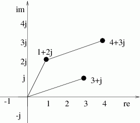
This is similar to the way vectors work. Indeed, complex numbers can be represented as vectors on an Argand diagram.
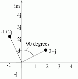
The operator × j can be interpreted as a 90 degree clockwise rotation. e.g., j(2 + j) = -1 + 2j.
Additionally, j4 = 1.
As our complex numbers are vectors, we can represent them in polar form. z = a + bj = r(cosθ + jsinθ). If we use Taylor expansions, we can break this down to ejθ = cosθ + jsinθ. Thus, ejθ is a unit circle on the Argand diagram and a general complex number, z can be written as rejθ.
When adding and subtracting complex numbers, the Cartesian form must be used. When multiplying or dividing, either form can be used, but the polar form is more convenient.
AC is distributed over the National Grid as it is easy to change voltage and current levels via transformer action. When we refer to AC in electricity, we normally refer to circuits in which the voltages and currents are sinusoidal in waveform. The sinusoid is important as it is easy to generate with rotating machinery and addition, subtraction, scaling, differentiation and integration produces sinusoids of the same frequency (hence linear (RCL) circuits have all their sinusoids at the source frequency). Mathematically it's a good basis function to represent other waveforms (fourier analysis).
Phasors
An ac signal (voltage or current) changes magnitude from instant to instant. Sinusoidal quantities can be conveniently represented using rotating vectors called phasors. Linear circuits with energy sources at a given frequency have all voltages and currents oscillating at that frequency. We can use a phasor diagram that disregards frequency information and captures the phase and magnitude information only.
By convention, phasors rotate anti-clockwise, so if a phasor has a positive j, we say it leads by the given angle and if the phasor has a negative j, it lags by the given angle.
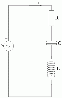
To discover the phasor of v, we can use KVL, so v = VR + VC + VL. These are vector quantites, so they must be added vectorly (e.g., using a vector diagram). In this circuit, we chose current to be the reference, as it is a series circuit and the same current flows through all 3 elements. The voltage across each element is different in voltage and phase, due to their different impedances. The phasor diagram then shows the phase relationship between the voltage and current. In this case, the current lags behind the voltage, as the inductive reactance is larger than the capacitative reactance.
As we know from complex numbers, we can represent an ac quantity by the phasor AejΦ, and this encapsulates both the magnitude (A) and phase (Φ) information.
Reactances
Now we have removed the dependance on time from our calculations, ac circuit calculations can be done with apparantely constant quantities, e.g., reactance calculations.
- V = IZ, hence
- ZR = R and also
- ZC = -j/ωc (= 1/jωc)
- ZL = jωL
Impedance
Impedance (Z) is the resistance to the flow of ac currents (the inverse of this is admittance, Y). Z may include:
- a non-frequency dependant part, called resistance (R). The inverse of this is conductance, G.
- a frequency dependant part called the reactance (X). The inverse of this is the susceptance, B.
V/I = Z = R + jX.
In general, X (a reactance) e.g., XC = 1/ωC and XL = ωL and ±jX is an impedance with 0 resistive component, e.g., ZC = -j/ωc and ZL = jωL.
Thus, resistances and reactances deal with magnitures, whereas impedances capture magnitude and phase.
From Ohm's and Kirchoffs laws, we can derive that series combination works such that ZS = Z1 + Z2 + ... and parallel combination works such that 1/ZP = 1/Z1 + 1/Z2 + ...
Frequency Response and Bode Diagrams
Often, we need to consider the behaviour of a circuit in the frequency domain, rather than the time domain, e.g., filters, resonant circuits, etc...
Any signal can be generated by the summation of sinusoids. These signals can be seperated using a filter (e.g., noise from a signal can be removed to isolate a particular frequency)
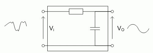
In the above filter, the filter gain is VO/VI
Low pass filters can clean up a noise contaminated signal after it has passed through a transmission medium. A high pass filter can remove DC between stages of transistor amplification, so transistor biasing is not affected.
Band pass filters can be employed which only allows signals of a particular frequency through.
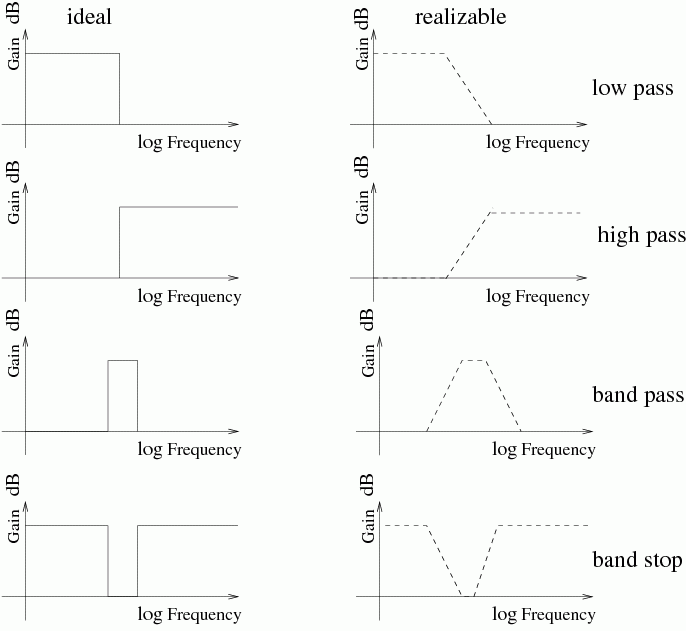
The effectiveness of filters can be shown by a graph of frequency against gain. Ideal filters of different types and a more realistic filter graph are shown below:
Frequency Response of Circuits
cos(ωt) → filter → G cos(ωt + Φ)
The system behaviour depends on frequency because reactances depend on frequency. This behaviour is known as frequency response. The frequency response can be measured by varying the frequency of the input signal and measuring the amplitude and phase of the output signal with regard to the input signal in steady state. The magnitude of the voltage gain, G, and phase difference Φ can be plotted as a function of frequency to describe the behaviour of the linear circuit.
Logarithmic Scales and Gain
Frequency and gain (but not phase) can vary over huge ranges, so we use logarithmic scales to represent these. A multiple of 10 of frequency is called a decade (similarly, a multiple of 2 is called an octave in music).
log10P is power P expressed in bels, however as this scale is very course, we use decibels (a tenth of a bel). 1 dB is 10log10P, which is power P represented in decibels.
As P is proportional to V2, 20log10V gives the voltage gain in decibels (derived from logarithmic laws, 10log10V2 = 20log10V.
0dB represents a unity gain (gain of 1) and negative dB represents attenuation. Gain can also be a phasor, G = Vo/Vi, therefore we can derive that G = GejΦ/ej0, therefore G = GejΦ, where Φ is the phase shift relative to the input.
Bode Diagrams
A Bode diagram is a method of representing frequency response. A Bode diagram plots gain and phase shift against f on two seperate diagrams. They are intuitive and easy to draw.
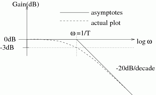
Since impedances are complex functions of frequency, a filters' behaviour can be described by a complex function of frequency. At certain frequencies (0 and ∞), the passive RC filters' gain and phase tends towards certain values (asymptotes). Constructing the Bode diagram requires drawing the asymptotes in a systematic manner.
If we take a simple example of a filter (Vo/Vi) we have a simple transfer function (from the voltage divider). This gives us Vo/Vi = 1/(1 + jωT).
We can find the asymptotes in the plot by finding where ωT << 1 and ωT >> 1. ωT << 1 ⇒ | Vo/Vi | ≈ 1, hence GdB ≈ 0 dB. ωT >> 1 ⇒ | Vo/Vi | ≈ 1/ ωT, hence GdB ≈ -20log10(ωT)
In this case, if frequency increases by a factor of 10, then log10(ωT) increases by 1, hence gain decreases by 20 dB - hence for sufficiently large frequencies, we have a slope of 20 dB per decade.
We also need to find the point where the two asymptotes meet - this is called the breakpoint. For first order low pass filters, the breakpoint defines the bandwidth of the filter. If Zc = 1/jωC, there may be no breakpoints. In our example, the breakpoint is where neither ωT << 1 and ωT >> 1.
For our sample Bode diagram, we can plot:
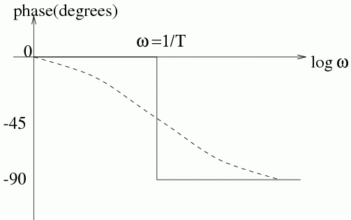
For the phase plot, we can also consider the cases at the asymptotes, which gives us Φ ≈ 0° for ωT << 1, Φ ≈ -90° for ωT >> 1. At the breakpoint ωT = 1, Φ ≈ -45°, so the phase plot looks as follows:
In addition to Bode diagrams, sometimes Nyquist diagrams are used. A Nyquist diagram represents frequency response by plotting gain and phase shift against frequency on the same graph. It is the locus of the endpoints of the output phasor for an input of Vi = cosωt as ω is varied from 0 to ∞. This kind of analysis is useful for control systems analysis.
Resonant Circuits
A mechanical example of a resonant circuit is a mass on a string (pendulum) that osciallates at a natural frequency (dependant on factors such as mgh) regardless of the force exerted. In this example, energy is repeatedly transformed between different forms (gravitational potential and kinetic, with a small amount of heat from friction) - this is typical of resonant circuits.
In resonant electrical circuits, energy is transferred between the electic field of a capacitor and the magnetic field of an inductor. The energy that is taken from the supply and transferred to heat is dependant on the resistance. The peak amplitude is dependant on the circuit resistance, which is analogous to the effect of friction on the mechanical system.
Sometimes resonance is to be avoided, particularly in mechanical systems, where it can be a destructive force. Other times, it is desirable, such as in frequency selective or tuned circuits. In practice, such circuits can be considered as narrow bandpass filters. The higher and narrower the peak in the response, the better the frequency selectivity. Selectivity depends on the resistance in the circuit, and this is referred to as the Q factor.
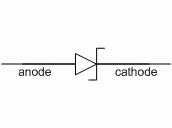
Diodes
RCL elements are linear (i.e., Vin ∝ Vout), however a diode is non-linear and therefore doesn't obey Ohm's Law (it's resistance is undefined). Diode circuits therefore don't have a Thevenin equivalent, and superposition doesn't hold.
![]()
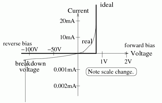
10 mA or more flowing through a diode (from the anode to the cathode) gives a voltage drop of about 0.6 V. The reverse current is negligable unless the reverse breakdown voltage is reached (a typical breakdown voltage is 75 V). The diode may be thought of as a one way conductor that has a small voltage drop across it when conducting.
Applications of Diodes
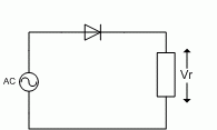
Rectifiers
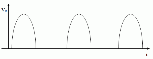
A half-wave rectifier can be made using a single diode.
This would give a wave form similar to:
Using four diodes, a full wave rectifier could be made:
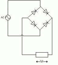
Which gives us a the following waveform:
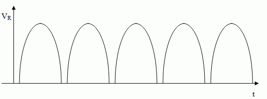
The gaps in between is caused by the small voltage drop that occurs through each diode. In the half wave rectifier, this is 0.6 V, due to their only being one diode and in the full wave rectifier, the drop is 1.2 V as the wave passes across 2 of the 4 diodes.
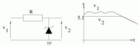
A crude DC power supply could be made using a full wave rectifier combined with a capacitor to smooth the waveform and a further regulator (such as a Zener diode) to smooth the waveform out further.
Diode Clamps
Diode clamps are often built into the inputs of CMOS chips to help prevent static electricity discharges occur during handling.
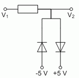
Here, when V1 goes above 5.6 V or below -5.6 V, the appropriate diode will start conducting, limiting V2 to 5.6 V or -5.6 V
Zener Diodes
Zener diodes have similar characteristics to normal diodes, except they are designed to start conducting at a specific voltage in reverse bias. Thus, when they are reverse biased, they can create a constant voltage in a circuit, derived from a higher voltate in a circuit. This process is called regulation, and this can be easily quantified and measures how the output voltage changes for a given change in input and how much dampening occurs. An ideal Zener diode has a regulation of 0 and has the following V/I characteristic graph:
Transistors
The transistor is the most important example of an active component. Unlike passive components, active components can have power gain, with additional power coming from a power supply. Transistors allow us to build many types of circuits, such as amplifiers, oscillators and digital computers (as ICs consist of a large number of transistors).
The transistor is a three terminal device in which either the current (BJT) or voltage (FET) in one terminal (the control electrode) controls the flow of current between the remaining two terminals by altering the number of charge carriers in the device.
When designing an amplifier using transistors, we are interested in the basic properties of:
- gain, which tells us how much output we get for a given input
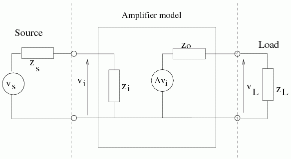
- input impedance, this, along with output impedance tells us about the loading effects through the voltage divider effect when we connect one circuit to another
For a good amplifier, Zi >>> Zs and Zo <<< Zl (except in power matching RF circuits, when we want Zi = Zo)
In electronic design most transistors are already implemented in the form of ICs, however knowing about transistors is useful as:
- the inputs and outputs of ICs are the inputs and outputs of transistors (open collector, etc)
- transistors are powerful interfacing tools between one circuit and another
- often, the right IC doesn't exist for a task
- someone needs to design the ICs in the first place!
Field Effect Transistor (FET)
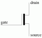
A FET takes virtually no current into the gate and the drain-source current is controlled by the gate-source voltage.
BJTs have a larger gain than FETs, so BJTs are usually used for simple single stage amplifiers. However, the FET operates with no forward biased functions, so no gate current is needed. FETs are much easier to use than BJTs. They have extremely high impedances, so no base current is needed.
In JFETs, the GS junction should be reverse biased to prevent conduction. For MOSFETs, there is no junction. The gate can be positive or negative with regards to the source.
The drain voltage of FETs are more nearly constant than the collector currents of BJTs for varying the voltage across the drain-source/collector-emitter. Additionally, unlike a BJT, a FET can be made to behave like a voltage controlled variable resistor.
Bipolar Junction Transistor (BJT)
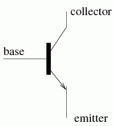
In a BJT, a small base current flows, which controls the larger collector-emitter current.
Further subdivisions of the transistor exist, depending on construction and the charge carrier polarity (holes or electrons).
![]()
In this course, we will be looking at npn BJTs and n-channel FETs.
For the npn BJT, the following rules apply for circuit design (the signs can be reversed to get the rules for pnp):
- The collector voltage must be more positive than the emitter voltage
- The base-emitter and base-collector junctions behave like diodes, with the base-emitter forward biased and the base-collector reverse biased
- The max values for current and voltage for the junctions should not be exceeded
- If rules 1-3 are obeyed, then IC = β IB, where β is the current gain, however, a circuit that depends on a particular value of β is a bad circuit, as β can vary from transistor to transistor.
BJT characteristics
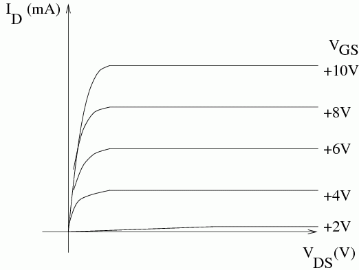
The V-I characteristics of a BJT collector varies according to IB, as the following graph shows:
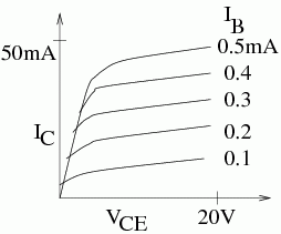
In an ideal transistors, the lines would not be curved, and would be straight across.
The transistor is approximately a controlled current source, but where is the output? If you pass the collector current through a resistor, the voltage drop across the resistor is proportional the the collector current, giving the voltage amplification that is needed.
Applying KVL to the circuit gives us VCC = ICR + VCE, or IC = -VCE/R + VCC/R. Using this, we can apply y = mx + c, where x = VCE and y = IC, so it can be plotted onto the characteristic graph above. This is called the load line, and has a slope of -1/R and crosses the axis at VCC/R. The load line is defined by setting appropriate valyes of VCC and R. As IB varies, the instantaneous values of voltage and current for the transistor collector-emitter slide up and down the load line.
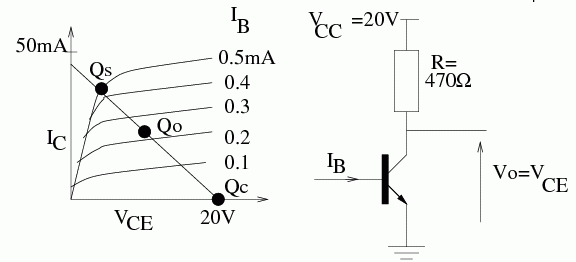
- QC is the cutoff point, where there is 0 collector current (no base current supplied)
- QS is the saturation point, the maximum transistor current, with the collector a tenth (or so) of a volt above the emitter
- QO is the operating point, working point, or the quiescent point. The region of the load line around this point is called the active region, where the best amplification can be achieved.
The first two states are extreme states, which are important when transistors are used as switches (i.e., in digital electronics, where the aim is to get it to switch between the two extreme points as quickly and as efficiently as possible). In analogue electronics, the active region is important.
Emitter-follower (BJT application)
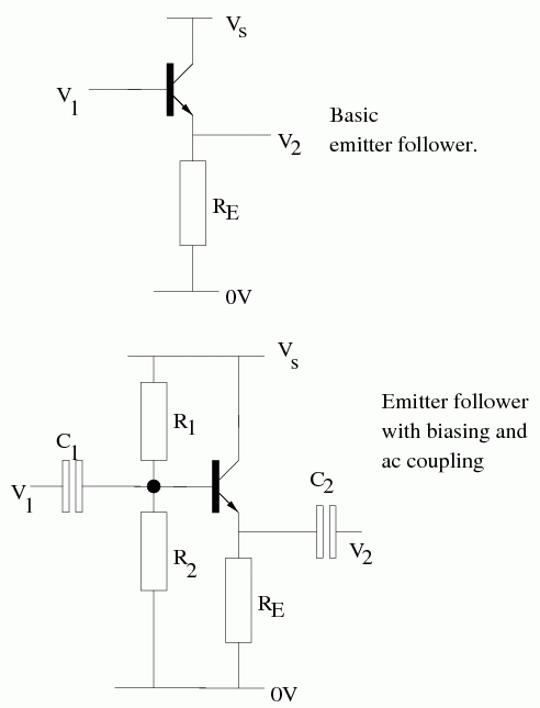
This circuit gives an output that is 0.6 V lower than output, and clipping occurs when V < 0.6. This circuit has a high input impedance, so it is useful as a buffer. They are most commonly seen as in the second diagram, where R1 and R2 set the biasing point and the capacitors remove any dc noise that may be introduced into the circuit.
Common emitter amplifier (BJT application)
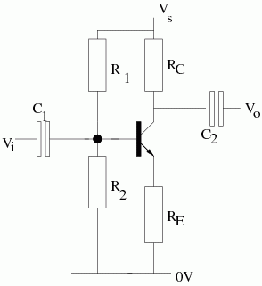
In this circuit, VO/VI = -RC/RE
FET characteristics
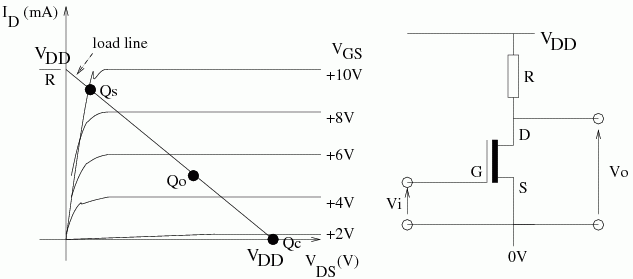
On the above I/V plot, for sufficiently high values of VDS, the characteristic is nearly horizontal and so only has a small dependence on VDS. However, the value of I is dependent on VGS. This makes the device a voltage controlled current source/sink.
If we want to produce a device that amplifies a voltage signal, we pass the DS current through a resistor connected to the drain of the FET. The output voltage must lie on a load line which is obtained from an application of KVL:
I = -VDS/R + VDD/R
The straight line formula (y = mx + c) can be applied, where y = I, m = -1/R, x = VDS and c = VDD/R.
The load line can be defined by setting appropriate values of VDD and R, then, as vGS varies, the instantaneous values of voltage and current for the transistor drain-source slide up and down the load line. When no signal is applied to the circuit, VGS must be biased to be roughly in the centre of the load line.
Self-Biasing Schemes
Rather than manually biasing a transistor, it is often simpler and more elegant to use self-biasing schemes, e.g.,
- JFET (n-channel) biasing - the GS junction is reverse biased. AC couple the input and put a resistor between the gate and ground. DC current through the source resistor sets the appropriate VGS.
- MOSFET (as with BJTs) requires a divider from the drain supply. Gate biasing resistors can be large (> 1M Ω), because the gate current leakage is so small (in the nanoamps).
Small Signal Analysis
Small signal analysis involves modelling the transistor as an ideal voltage source of gmvgs in parallel with resistance rd.
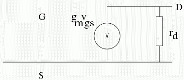
Current is a function of the gate-source and drain-source voltage and the change in current can be expressed as di = δi/δvGS + (δi/δvDS)δvDS. For small signals, we can write i = gmvGS + (1/rd)vDS, where the transconductance gm and drain resistance rd are marginally depedent on the operating point.
When analysing transistor circuits, we consider DC and AC seperately. DC values are indicated by upper case symbols and small signal AC values are indicated by lower case symbols. We consider DC first and get the biasing right, since AC properties have a small dependence on the position of the operating point in the transistor characteristic. We may then examine the transistor characteristic and the circuit diagram to determine AC behaviour, represented by the small signal model. DC sources are shorted to ground to form the small signal model.
Operational Amplifiers
The operational amplifier (op-amp) is a very high gain dc-coupled differential amplifier. It is a macro-component typically consisting of 10s of transistors packed into an IC.
An op-amp is designed to have a set of specific properties (most importantly, high gain) so that by choosing suitable feedback arrangements, the amplifier can be designed to carry out certain operations on the input signals, such as:
- amplification
- filtering
- differentiation/integration
- summation/subtraction
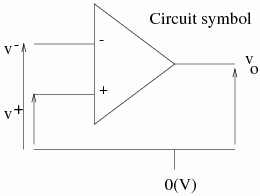
The op-amp is a high-gain differential amplifier with output vo = Av(v+ - v-, where Av is the gain, v+ is the voltage at the non-inverting input and v- is the voltage at the inverting input.
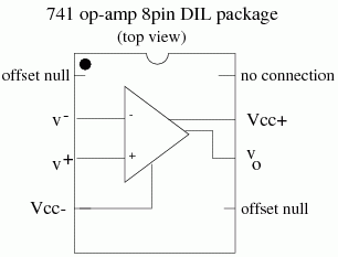
For op-amps, supplies of ±15 V are usually used (exact specs depend on the chip). The 741 op-amp will work from ±3 V to ±18 V.
Even with no signal applied to the op-amp, typically 1 mV will be at the input and if the voltage gain of the circuit is 1000, this gives a 1 V output for no input. To get round this, in an ac circuit, a coupling capacitor could be used at the output to remove the dc and for dc, the offset null circuit could be used.
Ideal Op-Amps
The ideal op-amp has characteristics such that:
- Gain Av is infinite
- Bandwidth is infinite
- Input impedance is infinite
- Output impedance is zero
From these ideal properties, we can infer the following principles:
- In a negative feedback arrangement, the output attempts to do whatever is necessary to make the voltage difference between the inputs 0
- The input draws no current
Ideal properties are often used in circuit design and analysis, but they should be justified in relation to other values in the op-amp circuit.
Negative Feedback (Inverting) Op-Amp
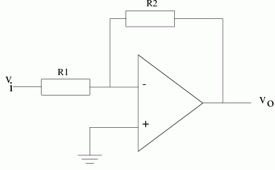
According to our ideal rule 1, the non-inverting input is earthed, so the inverting input must be at the same voltage (0 V). This point is referred to as a virtual earth. Using rule 2, the current into the inverting input is 0, hence applying KCL, we have: vi/R1 + vo/R2 = 0, which can be rearranged to give vo/vi = -R2/R1.
The previous expression can be generallised by replacing the resistances with impedances and replacing them, for example, with filters.
Non-Inverting Op-Amp
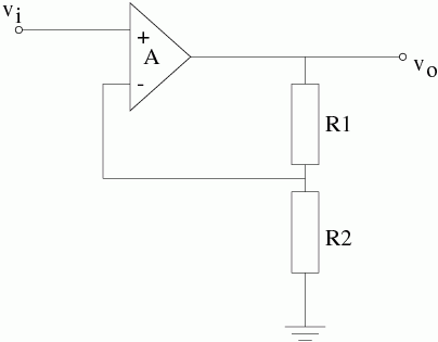
Here, v- = R2/(R1 + R2) × vo. The ideal op-amps means that v- = v+ = vi.
In order to judge which is the most appropriate op-amp configuration to use, we need to consider input impedance in addition to gain and phase shift considerations.
For the inverting circuit, the input resistance is R1, however in the non-inverting circuit, for our ideal op-amp this is infinite, but in the real world this is not the case. By doing a parallel combination of resistances, combined with gain, we can get a very large value, which is unpredictable due to A.
Feedback
From the basic equation vo = Av(v+ - v-), we can see that any signal vi = v+ - v- will almost immediately send the output into positive or negative saturation (i.e., close to one of the supply voltages). Thus, in linear applications, the op-amp is used in a negative feedback configuration.
Negative feedback is the process of coupling some of the output of the system (vo) back to the input (v-) to cancel some of the differential input (v+ - v-). If we use greater amounts of negative feedback, the circuit characteristics become less dependent on the open-loop characteristics of the ampifier and more dependent on the feedback network itself. Thus, in the ideal op-amp analysis, circuit properties are defined by input and feedback circuit elements only.
The open loop gain is when there is no feedback. When we do have feedback (normally through a network of resistors), we have closed loop gain. Closed loops give us constant gain up to the bandwidth limit. You need to take care when designing a circuit to ensure that the gain is in the graph area.
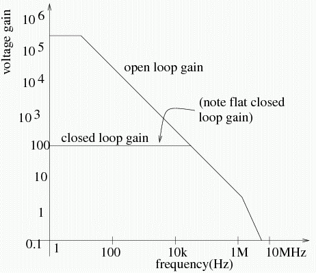
The unity gain bandwidth, fT, will be quoted for a specific op-amp. This is the frequency when the gain drops to unity and is also called the gain-bandwidth product.
The closed loop gain of the inverting amplifier circuit begins dropping when the open loop gain approaches R2/R1. This means if we have set R2/R1 to give a gain of 100, this gain may be limited by the open loop gain of the op-amp above 50 kHz. Indeed, for all amplifying/filtering applications, we must design inside the open-loop characteristic.
Non-Ideal Op-amp Analysis
| Parameter | Ideal values | Typical real values (for a 741 opamp) |
| Open loop gain | ∞ | 105 |
| Gain-bandwidth product | ∞ Hz | 1 MHz |
| Input impedance | ∞ Ω | 1 MΩ |
| Output impedance | 0 Ω | 100 Ω |
For a non-ideal op-amp, we can generalise resistances to impedances and add in the effects of finite input impedance and non-zero output impedance to the inverting amplifier circuit.
KCL can be applied at the inverting input and if we assume that the current taken by the load is negligable, we can apply KCL at the op-amp output. We can cancel out the value of v- and then if we have a much larger impedance at Zi then at Z1 and a much smaller magnitude at Zo then at Z2 we can get a formula for the gain: vo/vi = AZ2/(Z1(A + 1) + Z2) = -Z2/(Z1 + (Z2 + Z1)/A). If we have a very large A compared to |(1 + Z2/Z1)| we can further generalise to vo/vi ≡ -Z2/Z1. So we can apply ideal analysis to an op-amp inverting circuit, as long as:
- A >> |(1 + Z2/Z1)|
- |Zi| >> |Z1|
- |Zo| << |Z2|
Filters
Filters seperate signals of different frequencies by attenuating signals of all unwanted frequencies. They are often used to remove noise, which is present at all frequencies. To maximise the signal-noise ratio (SNR), we restrict the bandwidth of a circuit to the minimum necessary to allow the frequencies contained in the signal to pass and to filter all the other frequencies. An ideal filter is the "brick-wall" filter of rectangular shape, which is not realisable in practice.
Depending on the application (which has a given accepted and rejected frequency separation) we require the cut off to have a given steepness of slope. The corner should be as sharp as possible, i.e., rapid transition from pass-band to roll-off.
Simple passive RC filters produce gentle roll offs of 20 dB per decade. If a steep roll-off is required, we could cascade multiple low-pass filters. However, passive filters give us quite heacy dampening (ξ). Comparing the equation for cascading passive filters with the standard second order equation shows us ξ = 1, therefore Q (the quality factor) = 0.5, giving a large dampening and a "soft knee" in the frequency response.
We've already looked at LC resonance response, so we can use LC filters to reduce the dampening and give a sharper knee to the filter. By cascading LC(R) filters, we can have arbitarily steep falloff and corner sharpness, but a large number of components are required and inductors are bulky, expensive and can pick up interference (e.g., mains hum).
An op-amp with R and C elements can simulate the behavior of an LCR filter. Such a filter is called an active filter. Furthermore, due to the large input impedance and low output impedance of op-amps, loading problems experienced with cascaded passive filters are removed.
Sallen-Key Filter
The op-amp and voltage divider arrangement form a non-inverting amplifier G = K and where 1/2πRC defines the cutoff frequency.
As this is a non-inverting amplifier, vo = Kv3. We can then figure out the voltage divider effect for v3 and then use KCL round node v2. We can combine this three equations to give us: vo/vi = K/(1 + (3 - K)jωRC - ω2R2C2).
When K = 1, this is identical to a low-pass filter. As K increases from 1 to 3, decreasing amount of negative feedback has the effect of reducing dampening and giving a sharper knee. Note that by setting K = 3 we can eliminate dampening altogether - this gives us an oscillator!
As this is an op-amp, we don't have loading problems and stages are easy to cascade.
Non-linear Applications of Op-Amps
In linear applications, negative feedback pre-dominates. Even if some positive feedback is used, negative feedback must dominate for stability, the exception being sine wave oscillators, which are on the cusp between stability and instability and postive and negative feedback are perfectly balanced.. In non-linear applications, we may have no feedback (for comparators), or positive feedback (oscillators and Schmitt triggers). Here, the output switches to close to the power rails. It is important to note we can not assume v+ = v- for these applications, as negative feedback is required to enforce this condition.
Comparators
The comparator is used to determine which of two signals is larger, or to know whether a signal has exceeded a predetermined threshold. Ordinary op-amps are frequently used as comparators, but a slow slew rate gives a relatively long switching time (20 µs for a 741) due to stabilising internal compensation. The 748 op-amp has no internal compensation and a switching time of less than 1 µs, which is still too slow for many logic circuits.
The 311 comparator has a single rail supply and an open collector output (hence requiring a pull up resistor). This is an example of a special IC that are intended to be used as comparators and can move in and out of saturation much faster. However, comparators chips can not be used in the place of an op-amp, as they can be unstable in negative feedback arrangements due to a lack of compensation.
A simple comparator circuit has a slow output swing and multiple triggering, which is very bad for sequential logic, such as counters.
Connecting Rf introduces positive feedback and introduces dual thresholds, one for each output state. Positive feedback also gives us faster triggering. The resulting hysteresis ΔV is given by ΔV = R1/(R1 + Rf)Vpp, where Vpp is the peak-to-peak voltage change.
This is called a Schmitt trigger, and a graph showing the difference between a Schmitt trigger and a standard comparator is as follows:
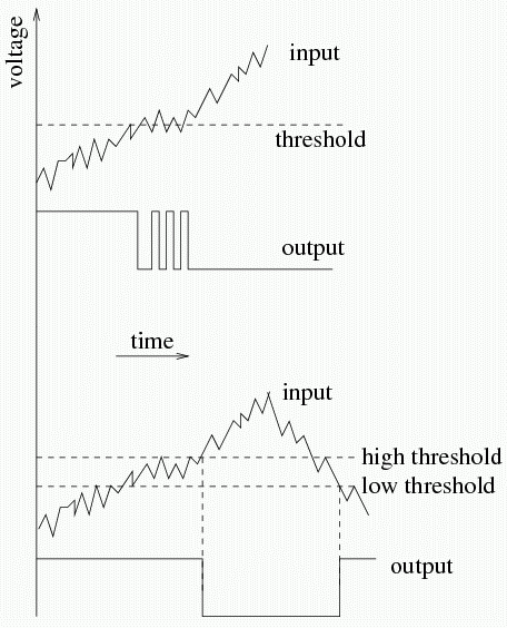
Oscillators
Op-amps can use positive feedback to generate signals (sine wave, square wave, sawtooth, triangle, etc) which can be used to drive electronic circuits.
As mentioned earlier, we can make an oscillator based on a Sallen-Key filter with K = 3.
The above diagram is that of a Wien-Bridge oscillator, which is popular for generating audio frequencies. The frequency generated is 1/2πRC.
Charging and discharging an capacitor between two threshold voltages combined with a comparator op-amp gives us a relaxation oscillator.
Digital/Analogue Interfaces
Computer control of analogue processes is widespread. Hence, we need a method to convert analogue signals to digital and digital signals to analogue.
Digital-to-Analogue Conversion
By changing the values of the resistors, you can weight each bit given its place weighting and the outputs are summed using an analogue adder (an opamp). These are difficult to fabricate on ICs due to difficulties in fabricating resistors with an exact value of R, but it is easier to make identically matched ones. Hence, DACs employing an R-2R ladder network are used.
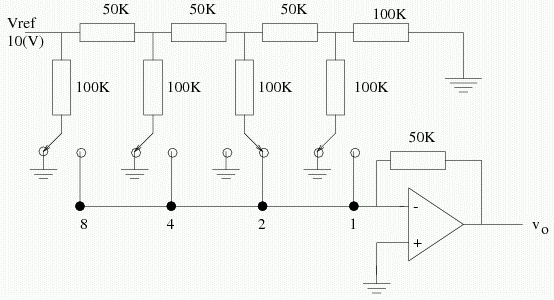
This circuit transforms binary scaled currents to an output voltage. The resistors must be precisely matched. It outputs 0 V for 0 binary input and -150/16 V for a maximum binary input of 15.
Analogue-to-Digital Conversion
Analogue signals vary continuously with time. When converting an analogue signal to a form that can be used by a computer, we require a digitsed, discrete time signal. The signal is sampled at a given frequency to give us a discrete time signal. The discrete time signals are digitised, i.e., they are represented by a fixed number of bits and so are quantised representations of the original analogue signal. The diagram below is an example of such a "sample and hold" waveform.
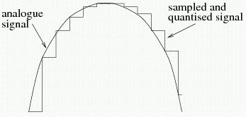
Nyquist Sampling Theorem
The sample-and-hold waveform can be low-pass filtered to remove the sharp edges and we effectively reconstruct the original waveform. However, we need to ask ourselves how rapidly do we have to sample in order to get an accurate reproduction of the original signal?
The Nyquist sampling theorem states that the sampling frequency, fs should be a minimum of twice the highest frequency content of the signal: fs ≥ 2fmax. If this is not observed, a distortion occurs called aliasing results. A graph showing the results of aliasing is below:
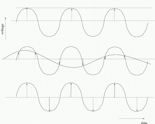
Analogue signals are often passed through a low pass anti-aliasing filter to ensure no frequency components higher than fs/2 are present when the signal is sampled.
Quantisation Error
If we wish to digitise a sinusoidal signal of amplitude V, then n bits must represent a voltage swing of 2V. A change of 1 in the binary representation of the voltage then represents: ΔVq = 2V/(2n - 1) ≡ V/2n - 1. More bits can be used to reduce the quantisation noise.
Several different types of ADCs are available and the correct choice depends on the application - whether speed or accuracy (i.e., number of bits) is required.
Flash Convertors
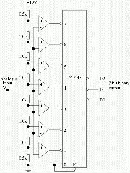
Flash convertors are fast (in the range of ns) and are typically used for video signals. Many parallel comparators are used to measure the analogue signal, one for each possible digital value. A binary encoder generates a digital output corresponding to the highest comparator number activated by the input voltage.
Typically only 8-bit accuracy is used. An 8-bit convertor requires 255 comparators. A 16-bit version would require 65535 comparators, which is unwiedly.
Single/Dual Slope Integration Model
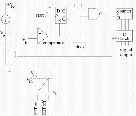
The single and dual slope integration methods let the capacitor charge up and is then connected to a comparator that stops a counter counting when the capacitor reaches a certain level. The dual slope method additionally can time the time for both charging and discharging.
The above diagram shows the single slope method.
Successive Approximation/Tracking ADC
![]()
A comparator is used to compare the analogue input with the digital output presented by an up/down counter. A negative feedback loop is then used to track the input.