The CPU
A CPU is a processing circuit that can calculate, store results and makes algorithmic decisions. It is this latter factor that sets computers apart from calculators.
There are different CPU types, including:
- register machines
- accumulator machines
- stack machines
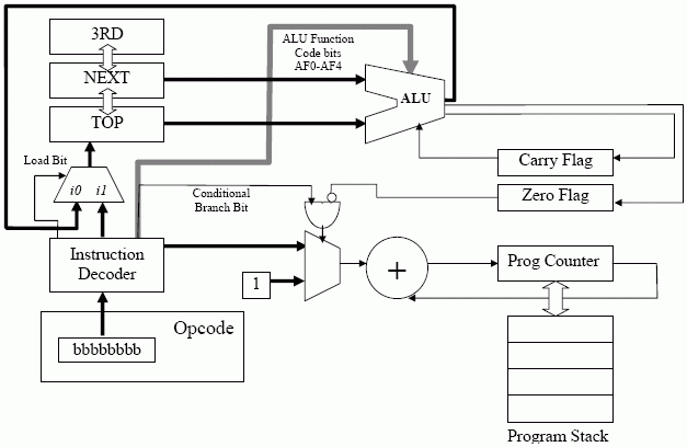
A very simple processor could be Jorvik-1, an accumulator machine:
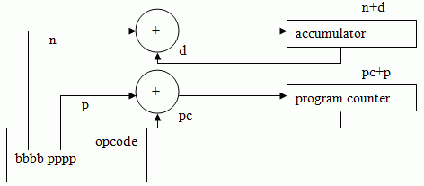
The program counter is a register showing the current location in a set of instructions and the accumulator is where values are stored before and after computation.
An example set of instructions for this machine may be:
| Hexadecimal number | Assembler equivalent | Description |
| 31 | ADD A 03h | This is 0011 0001, so add 0011 and incremement the pc by 1 |
| F1 | SUB A 01h | Subtract (this is only possible if the accumulator understands signed numbers) |
| 05 | BRANCH 05h | The accumulator is not affected, but the pc increases by 5 |
| 01 | NOP | No operation, just continue to the next step (this can be useful for timing purposes) |
| 11 | INC A | Increment (really it's just add 1) |
| 00 | HALT | Don't increment the pc, and have no effect on the accumulator. |
However, what is wrong with Jorvik-1?
- The instruction set is very limited
- Is it actually useful?
What features should a CPU have?
- Ability to perform operations
- Add
- Subtract
- Possibly other operations
- Ability to choose what part of program to execute next
- Branch always
- Branch conditional
- Ability to access and alter memory access - with one register, auxilary memory access is essential
Most CPUs have many more features than this.
Jorvik-1 can not conditionally branch, or access memory, so it does not fit into these features.
Let's consider an improved processor - Jorvik-2.
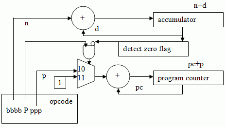
Here, we have changed the format of the opcode, reducing the maximum size of a branch, but allowing conditional branching. When P = 0, the branch is always taken (pc = pc + ppp), however if P = 1, the branch is only taken if the accumulator = 0, otherwise the program counter is just incremented - so we now have a "branch if 0" instruction.
Complexity
Jorvik-2 is more complicated, so requires more hardware. If we consider the propogation delay in the gates, Jorvik-1 takes 25 ns per cycle (which works out as 40 MHz), whereas the same cycle on Jorvik-2 might take 70 or 75 ms, depending on specific implementation details, such as synchronisation between the accumulator and program counter stages. 75 ms is 13 MHz, which is a 3 times decrease in speed compared to Jorvik-1.
What does this tell us about complexity? Complexity is related to speed, therefore simple circuits run fast and complex circuits run slow. Jorvik-1 may be faster, but is not complex enough to be useful.
If a new feature is important and heavily used, the advantages may outweigh the speed cost. If the feature is only rarely useful, it may be a burden and slow down the whole CPU.
Addressing
Data can be held in memory and is normally organised into bytes (8 bits), words (16 bits) or double words (32 bits). Data can also be addressed directly as an operand in an instruction - for example ADD A 03h has an operand of 03h.
Instructions normally operate dyadically (they require two operands), e.g., ADD A 03h has two operands - A and 03h. Having only one register (A) is not ideal and is not suited to the frequent case of dyadic operations. We should consider whether more registers would be better.
Our Jorvik-2 design is an extreme example of an accumulator machine - all operations use the accumulator (A) and a secondary operand. Having more registers will make our CPU more useful. We have already discussed 0 (stack), 1 (accumulator) 2 and 3 register addressing in operands in ICS, but adding more registers means complex and potentially slower circuitry. Adding fewer registers is normally simple and fast, but it could lead to harder programming, perhaps producing slower circuitry.
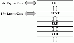
A Three Port Register File
Consider a three port register file of four 8-bit registers.
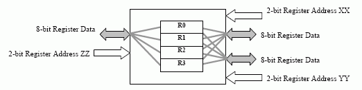
Accessing any three of these 4 registers simultaneously can create design problems. Reducing to two or one register addressing can ease the problem. Instructions must contain both the function code (ADD, SUB, etc) and the register addressed: FFFF XX YY ZZ - FFFF is the function code and XX YY ZZ are the registers (two inputs and an output) (as in the diagram above) - this is 10 bits long.
A One Port Register File
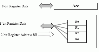
This is the standard accumulator model. It is much simpler, only one register file port is needed. Instructions contain one register address, the second register is always the accumulator. An instruction on this kind of machine looks like: FFFF RR - 6 bits long.
No Registers - The Stack Model
The stack (or zero-operand) model has no addressable registers, and thus no register file in the traditional sense.
Instructions only specify the function code (e.g., ADD, SUB, etc). Registers are always TOP and NEXT by default. An instruction in this model is only 4 bits long: FFFF.
We can implement a stack based on our Jorvik-3 machine, which adds an L (load) bit to the opcode which allows us to load something (a number bbb) onto the stack. However, we have lost a bit from our function code and introduced delays due to new components.
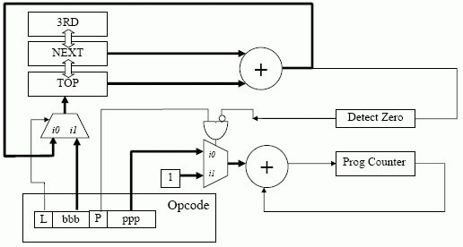
Upon examining Jorvik-3 we start to see some new instructions when we examine the circuitry. We have a new SET instruction which pushes a value onto the stack, and ADD, which adds two values from the stack together. However, our design only has a data adder in the path, so we can no longer do SUB. To get round this, we can SET a negative value onto the stack and then ADD.
Jorvik-3 has new features, however they come at a cost. We could work around this cost in various ways:
- making our instruction set 16 bit rather than 8
- improving the way branches are handled - most CPUs don't combine branches with arithmetic operations, and branch:arithmetic functions are in the ratio of approximately 1:6, meaning we're wasting about 40% of our bits in unused branches.
Having other functions would also be nice - a SUB function in addition to ADD, also AND and OR and the ability to DROP things off the stack would also be useful.
It would be difficult (not to mention slow) to introduce these features to our existing Jorvik-3 architecture, so we need another technology shift to Jorvik-4.
Instructions
Additional information is available on the instruction decoder on the CAR course pages.
The biggest advantage to the Jorvik-4 architecture over our previous architectures is that the opcode is now 8-bits long. We've already discussed what a CPU should have, but what other things are important in an architecture? Common sense and quantative data tells us:
- Speed of execution
- Size of code in memory
- Semantic requirements (what the compiler or programmer needs).
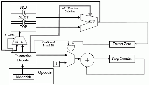
Decoding Instructions
Jorvik-1 through 3 used unencoded instructions - sometimes called external microcode. Each bit of the function maps directly onto internal signals.
The Jorvik-4 architecture uses an encoded instruction format. The 8-bit opcode is just an arbitary binary pattern, of which there are 256 possible permutations to decide which signals are to be applied internally. An internal circuit (the instruction decoder) does this, but wastes time doing it. There are two decoding strategies to use with an instruction decoder, either using internal microcode - a ROM lookup table that outputs signals for each opcode or hardwired - a logic circuit that directly generates the signals from opcode inputs. Microcode is easier to change, but hardwiring is usually faster.
Whether or not we use microcode or hardwiring, there is going to be a decoding delay. Suppose an ALU operates in 20ns, but a decoder takes 10ns, that means each operation takes a total of 30ns, or 33 million operations per second. However, with a clever design, we can overlap instructions, so the decoder can start decoding 10ns before the ALU is due to end the previous operation, meaning that the new instruction will be ready for as soon as the ALU finishes.
An encoded instruction format relies upon an opcode of n-bits, and each permutation is a seperate function. However, it is often useful to sub-divide functions in the opcode. We also need to consider the frequent requirements for data operands. We could assume that any operands will be stored in the memory byte immediately following the opcode. ADD and SUB are 1-byte instructions requiring only one opcode byte, but SET is a 2-byte instruction, requiring opcode and operand.
At the moment, Jorvik-4 is only an architecture - there is no defined instruction set. From our earlier machines, we almost certainly need to include the following instructions:
| Instruction | Description |
| SET nn | Push nn onto the top of the stack |
| ADD | Add the top two values of the stack together |
| SUB | Subtract the top two items together (NEXT - TOP) |
| BRANCH nn | Branch back or forward by nn place unconditionally |
| BRZERO nn | Branch back or forward by nn places if zero is detected |
| NOP | No operation (normally included by convention) |
| STOP | Stop execution |
We can see here which instructions are 2 bits and which aren't.
Delays
In addition to the delay we saw introduced by the instruction decoder, there are also delays introduced by memory latency. These include a delay from fetching an instruction (instruction fetch, or IF), and also a possible additional delay caused by fetching an operand (data fetch, or DF).
Our timing diagram for a SET operation may look like:
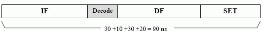
However, we can not assume that delays just add up to a final figure. Clocks usually have a uniform clock period, so our operations must be timed with clock ticks.
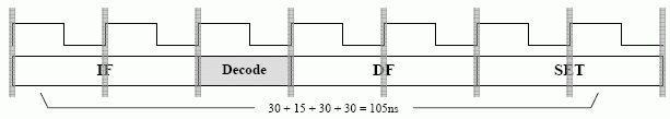
Here, decode is given 15ns, rather than the 10ns it needs and the operation execution has 30ns, instead of 20, leading to wasted time. A more sensible clock period may be 10ns.
Now that we've taken into account memory latency, we need to reconsider our overlapping time-saving technique. Only one fetch (instruction or data) can happen at once, so we need to wait for one IF to finish before starting the next one, but we can overlap the IF with the decode procedure and then overlap the decode as before. However, if the instruction is a two-byte instruction and requires a DF also, we're in trouble. We can't start the next IF until that DF has finished, and as the IF and decode operations take longer than the execution of operation, we still end up waiting, negating the effects of our overlapping. Therefore, we want to avoid 2-byte operations whenever possible.
SET is a frequent operation, but common sense tells us that frequent operations should be fast and compact, so we should look at ways to improve the performance of this command. Patterson & Hennessey tell us that at least 40% of constants are 4 bits or less, and 0 and 1 are very commonly used. We could improve matters in varying approaches:
- Maybe we could have a special short set instruction (SSET n as well as SET nn)
- A special "Zero" opcode could be used to initialise a zero onto the stack
- We could replace SET 01h, ADD with a special INC function.
- We could also replace SET 01h, SUB with a special DEC function.
If we decide to have a SSET function, we must consider how this would work in practice on an 8-bit instruction set. If we have XXXX dddd, this gives us 4 bits of opcode and 4 bits of data and SSET values 0-15. This is too restrictive, as we would only have 16 instructions available, each with 4 bits of data.
However, we could only have dddd when XXXX = 1111, so opcodes 00h to EFh are unaffected and we still have 240 possible opcodes, and then opcodes F0h to FFh give us SSET 0h to SSET Fh. As F0h is SSET 0h, we don't need a special "initialise 0" function any more.
The Stack
We covered the concepts of stack-based computing in ICS. Let's consider that we want to calculate the average of three numbers, X, Y and Z.
| Instruction | Stack Content |
| SET X | X |
| SET Y | Y X |
| ADD | Sum1 |
| SET Z | Z Sum1 |
| ADD | Sum2 |
| SET 3 | 3 Sum2 |
| DIV | Average |
Here, we've added yet another command - DIV, which divides. However, if DIV does 3 ÷ Sum2 instead of Sum2 ÷ 3, we have a problem.
Stack order affects a computation, so we should add commands that manipulate the stack.
- SWAP - this swaps the top two elements of the stack so X Y Z becomes Y X Z
- ROT - this rotates the top 3 items on the stack so X Y Z becomes Z X Y
- RROT - this rotates the stack in the opposite direction, so X Y Z becomes Y Z X
Re-using Data Operands
Say we have the formula (A - B) ÷ A, we can see that A is used twice, but in our current instruction set, this would require 2 fetches of A into our stack, and as every fetch introduces a delay penalty, this might not be the optimal solution. Using our current instruction set, an implementation of this may use 9 bytes of storage and 3 fetch delays.
We could implement a DUP operator which duplicates the top of the stack.
| Instruction | Stack Contents |
| SET A | A |
| DUP | A A |
| SET B | B A A |
| SUB | Sum1 A |
| DIV | Result |
| STOP |
This requires 8 bytes of storage and only 3 fetch delays.
Another useful command would be the DROP instruction, to throw away the top stack item, so X Y Z becomes Y Z, for example.
Another approach to stacks is orthogonality and scalability, of which more information is available in the original lecture slides.
Branches
All architectures have some form of branches. We could use them for:
- skipping over parts of a program - normally conditional
- jumping back repeatedly to a certain point (i.e., a loop) - normally conditional.
- moving to another part of the program - normally conditional
In cases 1 and 2, the branch will probably be quite short. In case 3, the branch distance could be quite large. According to Patterson and Hennessey, 50% of branches are ≤ 4 bits (based on 3 large test programs). These are almost certainly mostly types 1 and 2.
If all branch operations were 8-bit, we'd need 2 bytes for every branch and 2 fetches. However, if we have short 4-bit operand, then 50% of brances will be 1 bit only.
The most common type of branch is a relative branch - these are normally used within loops. They test a condition and loop back is true. Brances are used to skip over code conditionally.
Long Branches
Long branches are used to jump to another, major part of a program. Normal branches have a limited range, of about 27 (7-bits and a sign bit), so long branches use a fixed (absolute) 2-byte address (16 bits). Long branches get relatively little use, compared to other branching methods. Long branches have been replaced in a lot of cases by procedural code.
Indirect Branch
A memory address is given in the branch opcode. The memory address contains where to jump to, rather than the opcode. e.g., IBranch 06h would jump to the address stored at location 06h.
Such branching schemes are speciallised (sometimes called a jump table), but can speed up cases where there are multiple outcomes to consider (e.g., a 'case' in higher level programming languages). IBranch could also be implicit, using the value on the top of a stack.
ALU
The ALU is the Algorithm and Logic Unit. It is capable of monadic (1 operand) and diadic (2 operand) operations. The ALU requires operands and a function code (to tell it what to do).
The ALU is used for performing calculations (some are floating point, others integer only), manipulating groups of bits (AND, OR, XOR, NOT) and for testing conditions (test-if-equal, test-if-greater, test-if-less,test-if-zero, etc).
The ALU also has a carry flag which occurs when arithmetic takes place if the result is too large to fit in the available bits. The carry flag "catches" the final bit as it falls off the end.
Software vs. Hardware
A hardware multiply instruction may be very fast (1 cycle), but requires complex circuity. It can also be done in software using two methods:
- repeated addition: 10 × 3 = 10 + 10 + 10
- shift and add: 10 × 3 = (3 × 0) + (30 × 1)
Calls, Procedures and Traces
Programs consist of often repeated sequences, or 'routines'. An in-line routine is coded at each point when they are needed - this is inefficient on memory use.
In a real program, a common routine may be done 100s of times, so doing it in-line may result in an increased possibility of bugs. Complicated procedures may takes 10s or even 100s of lines of instructions.
How can we avoid this repetition? One answer is to branch to one part of the program and then branch back when finished. If we store this return value (where to go back to) somewhere, we know where we'll be going back to.
To implement this in our architecture, we need new instructions:
- CALL nnnn - this stores the current pc somewhere and branches to the specified address
- RETURN - this gets the stored pc value and branches back to that address (the stored pc value should really be the instruction after the original CALL, otherwise you would end in an endless loop).
We now have a smaller program with greater consistency in code, however the CALL and RETURN have overhead.
Hardware Considerations
To implement this, we need to consider how we will store the return value. One way is to just have a second pc register, which allows single level depth, but this is limiting. Adding a stack to the pc to allow multiple level calls (nested procedures) is more flexible. This is often called a program stack or return stack.
Now we need to consider how our instructions work. CALL would push pc + i (where i is the instruction length of the call operand - i.e., in a 16-bit address this would be pc + 3. Many architectures automatically increment the program counter after the instruction fetch anyway so often this isn't something to worry about) onto the stack and put the new address (operand of CALL) into the pc register. The machine then automatically goes to and executes the address in the pc.
For the RETURN instruction, the value on the top of the stack is popped onto the pc and the machine automatically follows this new instruction.
Traces
Traces are a useful hand debugging tool, especially for debugging loops. You act as the CPU, listing each instruction in order of execution, alongside the stack contents. From this you can check that the program behaves as expected, and possibly identify bugs in the architecture.
Long vs. Short
Usually CALL instructions have 16-bits (or longer) operands, however important routines - sometimes referred to as 'kernel' or 'core' routines - get called very often. These could be I/O procedures such as reading a byte from the keyboard or updating a display character or low-level routines such as multiply (if it's not implemented in hardware).
We could implement a 'Short Call' instruction, like SSet and SBranch. However, this gives us only 16 possible addresses. Each number should represent a chunk of memory, not a location, however - otherwise each instruction could only be 1 byte long.
Now our instruction set looks like this:
- F0 - FF SSet
- E0 - EF SBZero
- D0 - DF SBranch
- C0 - CF SCall
SCall 01 might call address 010000, SCall 02 100000, etc... - each address is bit-shifted so the instructions can be longer. If these addresses are at the beginning of memory, then SCall 00 is a software reset feature, as it runs the code at the very beginning of memory, rebooting the system.
So, implementing this in our new machine we get the final Jorvik-5, a dual-stack architecture.
However, additional hardware is required in the program counter path to figure out the new program counter value when incrementing in a call.
Addressing Modes and Memory
Addressing Modes were
also covered in ICS.
An addressing mode is a method of addressing an operand. There are many modes, some essential, others specific. We have already used several addressing modes, consider:
- SET nn - the operand is immediately available in the instruction, this is called immediate addressing.
- BrZero nn - the address we want is nn steps away, relative to the present pc value -this is relative addressing.
- LBranch nn - the address we want is nn itself - this is absolute addressing.
- Skip - this is implicit, there are no operands
Implicit
This is typical with accumulator or stack-based machines. The instruction has no operands and always act on specific registers.
Stack processors are highly implicit architectures.
Immediate
Here, the operand is the data, e.g., Set 05 or SSet 6h (here, the operand is part of the opcode format).
The Jorvik-5 could make better use of immediate instructions, e.g., ADD nn adds a value onto the stack, instead of SET nn, ADD. This operation is a common one, so it may be worthwhile to implement this, although it does require hardware changes. We can justify this change if:
- it occurs frequently
- it improves code compactness
- it improves overall performance
In our current Jorvik-5 architecture, an instruction might requires 70 ns to execute. In our new design, each instruction now takes 80 ns to execute, but constants can be added with only one instruction. Taking into accounts fetches, our immediate add is now 30% faster, but we have a 14% slowdown for all other instructions.
We need to consider whether this trade off is worth it. If we plot a graph of speed-up against frequency of immediate add's, we need 30% of instructions to be immediate add's for the trade-off to break even, and 50% to gain even a modest 10% improvement.
Absolute
This form of addressing is very common.
To implement absolute addressing in our architecture, we need some new instructions:
- CALL nn - we've already covered this
- LOAD nn - push item at location nn onto the stack
- STORE nn - pop item off the stack into location nn.
Relative
This is commonly used for branches and speciallised store and load. The operand is added to an implicit register to form a complete address.
This is useful for writing PIC - position independant code. This kind of code can be placed anywhere in memory and will work.
Indirect
This addressing mode is more speciallised and less common. The operand is an address, which contains the address of the data to be accessed (an address pointing to an address). This is sometimes called absolute indirect.
Register Addressing
This is common in register machines. Here, registers are specified in the operands, e.g., ADD A B. Stack machines also have registers, mainly speciallised ones (e.g., the pc or flags such as carry and 0)
Register Indirect
This is a mixture of register and indirect addressing. Here, the register contains the memory location of data and then it works like indirect addressing.
High-Level Languages
High-level languages were developed in response to the increasing power of computers. It was becoming harder to write correct programs as the complexity of the instruction set increases. High-level languages come in two main types:
- Compiled to target - high-level language statements are translated into machine code and the program is executed directly by the hardware. This method can generate large programs.
- Compiled to intermediate form - high-level language instructions are compiled into an intermediate form (bytecode) and these intermediate forms need to be executed by an interpreter. This method tends to product machine-independant compact programs, but the interpreter also needs to be present.
The main requirement for an interpreter to be supported at machine level is the ability to execute one of many routines quickly. Each 'routine' defines a function in the language semantics. Ibranch allows us to branch to one of many subroutines, so we could implement an interpreter control loop with this. Each bytecode represents a location in the jump table, so we can use this to decide where to jump to to implement the instruction.
Typical languages consists of statements which we need to support in our machine architecture such as:
- Variables and assignment
- Conditional statements (if-then-else)
- Case (switch, etc).
Managing Variables
A few values can be kept on the stack or in registers, however most high-level languages have 100s of values to deal with. Registers and stacks are too small to support this, so we have to use main memory. We could store our variables at fixed addresses (e.g., X is 1000, Y is 1001, etc), but this is difficult to manage and wasteful as not all variables are needed at all times. We could store this values on another stack, so when they are created they are pushed onto the stack and when they are finished they can be dropped off. This type of implementation is known as a stack frame.
Stack Frames
Stack frames are needed for variables, as these need to be created and deleted dynamically and we have to keep variables in memory. Arrays are also variables and as such have the same issues, but they can contain many seperate data items. We need to consider how to manage the storage of these items effectively.
We also need to consider the program structure, which might consist of procedures and nested calls, recursion and interrupts. We can also have multiple instances of a procedure as multiple calls to the same procedure can co-exist.
Stack frames help as variables can be added to, or removed from, a stack. The stack resides in memory, but it can be located anywhere. For an array, the stack can hold a few, or many, bytes just as easily. As for the program structure, the stack frame can store the context of each procedure - recursive calls to procedures cause the preservation of the previous state. Multiple instances can also be implemented in the same way, where each call has its own state on the stack.
If we assume that we have a new third 'allocation' stack in Jorvik-5, then when a procedure is called, the first thing that happens is that variables are declared and created on the stack. If we had a procedure with 2 variables, A and B and an array X of length 4, then A, B, X[0], X[1], X[2] and X[3] are pushed onto the stack, on top of any data already on the stack. If our program was recursive, then we could get many stacks on top of each other and each one will maintain the correct state. Nesting is essentially the same principle, but a different procedure is called.
Our stack architecture has to place data on the stack to do computations, but the variables are held in memory - how do we get them onto the stack? A way to accomplish this is using indirect addressing. If we know a 'top-of-frame' address, then we can work out the address of a variable in memory.
We need another register to store a pointer to the top of the stack frame, which can be pushed onto the main stack for computation of indirect addressing. Because of the regularity of this process, we could have an indirect load instruction (LOAD (TOF)+02), if we figure it increases performance, however this is deviating from the stack machine philosophy. This kind of instruction does exist in register-based CPU, such as the 68000.
In high-level languages, there are more to variables than this, however. We have currently implemented local variables, which are created a procedural state and destroyed after the return and can only be accessed by the program that creates them, however we also have to consider global variables, which are usually created before the main procedure and can be accessed by any procedure at any time. So, our frame stack has to be accessible in two parts, one for globals and one for our current procedure (locals).
We can use a stack to store our pointers, so when we return, our stack frame can be restored. With this stack of pointers, we can access variables from higher levels.
Conditional Statements
To deal with conditional statements, we put the values to be compared on the stack, and then use a test operation (which sets the 0 flag is the test is true) and we can then do BrZero
Case Statements
Here, an Ibranch is used with a jump table.
Arrays
Arrays are typically placed in memory (in a stack frame or elsewhere) and access to the array is computed by using indexes to figure the offset from the array start.
Compilers
As we stated earlier, compilers turn high-level language statements into low-level machine code by recognising statements in the high-level language such as if-then and case and then outputting predefined machine code fragments.
Based on the examples given in the lecture slides, we could write a compiler for the Jorvik-5 and with a little work, a program could be written to recognise common statements and output Jorvik-5 machine code. There are various complications and refinements to be made, however, but the basic idea is there.
Interrupts
An interrupt occurs when a device external to the CPU triggers an interrupt request line (IRQ). The CPU responds with an IRQ acknowledge when it has processed the interrupt. An interrupt is a request from a device to the CPU to perform a predefined task, called the Interrupt Service Routine (ISR).
However, if there are several devices, things get more complicated. One option is to have an IRQ line for each device, but this leads to lots of CPU pins. An alternative is to allow all devices to share an IRQ line, but then we have to consider how to safely share one line.
Shared IRQ Approach
We have to somehow combine the IRQs from each device to signal an interrupt request. A tri-state OR gate can be used for this, however if more than one device triggers an interrupt, how does the CPU know which device needs servicing?
We can use the idea of interrupt prioritisation to work round this. A device has the idea of priority, and can only raise an interrupt if there are no more important devices requesting one. A method of implementing this is using daisy chaining, where a more important device in the chain lets the one directly below it know whether or not it (or any devices above it) want to use the interrupt, so the permission is passed down the chain. A single acknowledge line is used, with each device connected in tri-state. Only the device that generated the input pays attention to it.
However, we still have the problem of knowing which device initiated the interrupt, and which service routine to run.
Vectored Interrupts
To implement this, we can use vectored interrupts:
- A device triggers an interrupt
- The CPU acknowledges for more information
- The device issues a byte on the data bus
- The CPU reads the byte
- The byte can be an opcode, or vector address (jump table) - the exact details are architecture specific.
In Jorvik-5, we can use opcode interrupts where the short call uses a subroutine with I/O info. Each device has a different bit pattern for different opcodes. Negotiation is needed to ensure the correct subroutine is called.
Fully-Vectored Interrupts
If a single opcode is > 1 byte, then opcodes are tricky. A vectored address contains part of address with a subroutine in - e.g., an 8-bit vector (the VPN - vector page number) is combined with another 8-bit number (the VBA - vector base address) to give us the full adress. However, to make full use of the 8-bits we can only have 1 location per routine, which is not enough to be useful. Real systems use an interrupt vector table. The CPN is shifted so each location is 2 bits longer, combined with a 7-bits VBA. We can then use indirect addressing for our ISR as the actual instructions are in the 16-bit memory location given.
There are also other considerations we should make. We never know when an interrupt is going to be called, so the present state of the CPU needs to be preserved when the interrupt is called, and the ISR also needs to leave the CPU in the exact state is was before it started, otherwise program crashes may occur.
History of Computing
Ancient History
Abacuses were the most basic form of computing, and were thought to be invented by the Babylonians or the Chinese in 1000-500 BC. Common abacuses use base 5 or 10, and binary did not become the standard until the 1940s. In computing, binary is more stable, and less susceptible to noise (being either on or off, not laying inside certain band limits).
Charles Babbage (1791-1871)
Babbage is widely recognised as the father of computing and is most famous for designing the difference engine and analytical engine.
Difference Engine
The difference engine was commissioned by the British government to provide accurate logarithmic, trigonometric and other tables for their seafaring merchant and naval vessels. It could be considered to be an application specific computer (ASC) (i.e., optimised to provide one specific task). It worked by evaluation polynomials using the method of finite differences.
One of the main aims of the project was to cut out the human computer, thus removing any errors, therefore, the system needed to be able to print out the results to avoid any transcription errors - much like current times with automatic code generation.
The Difference Engine was constructed from a set of mechanical registers (figure wheels) storing differences Δ0 yi, Δ1 yi, ... and adding mechanisms and had eight storage locations with 31 decimal digits.
High levels of accuracy were required to minimise the effect of accumulated errors i.e., 31 decimal digits is equivalent to 103 bit arithmetic. Fractional numbers were multiplied by a constant i.e., scaled to fit within the machine�s integer representation and negative numbers were computed using complement notation.
To save cranking, and to speed up operations, the Difference Engine could be set for parallel "pipelined" operation. The maximum speed of the Difference Engine was 10 calculations a minute, or a result every 6 seconds. An attempt to run the system faster than this the momentum of some parts caused the transmission mechanism to bend, resulting in jamming or broken gear teeth.
In summary, the difference engine had register storage, addition with a ripple carry mechanism, a pipelined architecture and was capable of parallel operations.
Analytical Engine
Charles Babbage designed his analytical engine, which was the first programmable general purpose computer (although not stored program), however he never built it, due to lack of funds. It used microcode for complex operations. It was a lot bigger than the difference engine, and some designs went as far as 50 registers and 40 digit precision.
The main innovations were the seperation of storage and calculation units, giving us the Store (V) and the Mill, containing accumulators (A). Operations were controlled by the programmable card (consisting of operations cards, variable cards and number cards), and was based on the Jacquard loom. Babbage suggested using a printer, punched cards and a curve drawing machine as outputs, giving the machine both inputs and outputs.
The Analytical Engine used look-ahead carry, speeding up addition considerably (into a constant, rather than linear based on the length of the number), but 10 times more machinery was used for the carry than for the addition.
Electromechanical Machines (First generation relay and valve machines)
Konrad Zuse (1910 - 1995)
After Babbage's death, no serious attempts were made to build a general purpose computer until the 1930's. The first examples (the Z1 and Z3) were discovered after WWII and were found to be built in Germany between 1936-1941.
The Z1 machine represented numbers in a 22-bit floating point format and the arithmetic unit was an adder only (therefore subtraction could occur using complement notation) and all operations had to be reduced to addition. However, it was not very reliable, so the Z3 was constructed, which was made entirely out of relays and was programmed using punched tape and a user console.
The Z3 used microcode implemented using a micro sequencer constructed from stepwise relays and instruction overlapping was used (see earlier in notes - an instruction is read whilst result of last one was being written). A look-ahead carry circuit was constructed from relays which allowed fast addition to occur.
Harvard Mk I
The Mk I was developed by Howard Aiken and was built by IBM between 1939 and 1944. It was also known as the IBM Automatic Sequence Control Calculator (ASCC). It was constructed from electromechanical relays, was 55 feet long, 8 feet high, 2 feet deep and weighed 5 tons, making it relatively slow and very noisy. Numbers of up to 23 decimal places could be represented using electromagnetic decimal storage wheels - 3000 of which were present in the machine. The Harvard Mk I was used by the US Navy for gunnery and ballistic calculations until 1959 but it was out of date by the time it was commissioned.
Aiken went on to develop the Harvard Mk II, III and IV using valve technology, and he also developed the concept of the Harvard computer architecture, which uses physically seperate instruction and data memory. This allowed the next instruction to be read whilst the previous data is being written to memory and the width of the address and data bus could be different and optimised to the appropriate size. However, two memory modules were now required and storing programs inside the instruction memory could be difficult.
This is used in modern systems, where it is important to isolate the path between the processor and memory to maximise performance. Nowadays, a dual independent bus (DIB) is used. This replaces the system bus with a frontside bus (FSB), connecting the system memory (via the memory controller) to the CPU, and also to the other buses. The backside bus (BSB) is used to provide a fast direct channel between the CPU and the L2 cache.
ENIAC
ENIAC (Electrical Numerical Integrator and Computer) used valve technology instead of relay technology, and consumed 180 kW of power. It was commissioned by the US Army to calculate firing tables for specific weapons for a range of environmental and weather conditions. It was completed in May 1944, and has a strong claim to be the first ever general purpose electronic computer (although this is a topic of much debate). It was developed by a team lead by JP Eckert and JW Mauchly and was decimal, using over 18,000 valves and weighing 30 tons. It was much faster than anything ever built previously, and multiplication could occur in under 3 ms. It was described as being "faster than thought".
ENIAC was not a stored program computer, and needed rewiring if it was needed to do another job. For each program, someone needed to analyse the arithmetic processing needed and prepared wiring diagrams - a process which was time consuming and prone to error. This led to people such as John von Neumann to develop the idea of storing programs inside the computers memory - von Neumann originally envisioned programs which could modify their own program and rewrite itself. This innovation was a major factor that allowed computers to advance. This architecture was called the von Neumann architecture.
The von Neumann architecture used the same memory for instructions and data. The advantages of this was that a single memory module could be used, minimising the number of programming pins and buses. Instructions and data were treated equally, allowing data to be easily embedded into a program. However, this required the bandwidth of the memory bus to double and optimisations made by having seperate data and address bus sizes were lost.
Manchester Baby
This is sometimes referred to as the Small Scale Experimental Machine and it was the first ever electronic binary computer which executed its first stored program on June 24th 1948. It was created by a team at the University of Manchester between 1947 and 1949 consisting of Turing, Williams, Kilburn and Tootill. It had a 32-bit word length and used serial binary arithmetic using two's complement integers. It had a single address format order code and a random access main store of 32 words - extendable up to 8192 words. The computing speed was about 1.2 ms per instruction. It used Williams' idea of data storage based on cathode ray tubes (a Williams-Kilburn Tube) as the main store. This CRT had a big advantage over existing memory (delay line memory) as it allowed fast, random access to short strings of bits (i.e., 20-bit or 40-bit). The bits were stored as electrical charges on the phosphor of the CRT and had to be refreshed roughly every 0.2 s.
Delay line memory worked by electrical pulses being converted to sound pulses and then being transmitted down a long tube of mercury. A sufficient delay allowed a number of bits of data to be stored before the first bit was received and then re-transmitted. This was slow, serial and didn't allow random access to memory.
The Manchester Mark I had the first hard disk - two magnetic drums used for backing store. It was relatively slow, but had 16 times the storage of the CRT memory. The Manchester Mark I wsa the first to use a paging type memory store, where memory was divided into pages, each one containing 32 40-bit words (the size of a basic Williams-Kilburn tube) and was used as the unit of magnetic drum storage. In the Manchester Mk I, there was 4 pages of RAM main store and 128-page capacity of the drum backing store.
Each 40-bit addressable line could hold either 1 40-bit number, or 2 20-bit instructions.
EDSAC
EDSAC (Electronic Delay Storage Automatic Calculator) was built by Cambridge University in 1949. EDSAC stood out from its contemparies as it added microcode to the architecture, rather than the previous method of hardwiring control methods.
Collectively, these machines are referred to as the first generation computers and they share a similar system architecture. A typical example of the first generation machines was the IAS - a computer designed by von Neumann. The other major architecture of the time was the Harvard architecture.
This generation introduced isolating the processor from the IO with a dual independant bus architecture, replacing a single system bus with a frontside bus (FSB) and backside bus (BSB).
Second Generation Computers (Early Transistor)
The second generation of computing brought a change from valve to transistor and lasted between 1955 and 1964.
William B Shockley has been termed the "father of the transistor". He joined Bell Labs in 1936 in the vacuum tubes department before moving to the semiconductor department. The transistor is equivalent to a three-terminal electrical switch (triode). early transistors - point contact - were difficult to manufacture and were also unreliable. A few months later, work started on the junction transistor. Compared to valves, these were smaller, more reliable, faster and required less power.
The first experimental transistor computer was built in Manchester in 1953. It used 200 point contact transistors, 1300 point diodes and had a power consumption of 150 W. Main memory was implemented using a drum store, meaning that the transistor computer was slower than the mark one. The design was used as the basis of the MV950 in 1956, which was built using the more reliable junction transistors.
The next advance in this generation of computing was the non-volatile ferrite core memory. Each core had a diameter of about 2 mm and two magnetising wires and one sense wire passed through each one. The cores were arranged in a matrix such that each location was addressable.
A current passing through one of the magnetising wires would set a core magnetisation which could then be detected. Passing a current through the other wire would reset the magnetisation, giving either 1 or 0.
Many computers in this generation were transistor/valve hybrids, or just transistor implementations of the older valve computers. Another key part of this generation was the development of index registers and floating point hardware, the use of dedicated IO processors and hardware to supervise input/output operations, high level programming languages such as COBOL, FORTAN and large scale computer manufacturers also supplying compilers, software libraries with their machines.
Third Generation Computers
The IBM System/360 is the system which defines this generation of system - the classic mainframe computer system.
This machine used Solid Logic Technology (SLT), which was a transition between discrete transistors and integrated circuits. The System/360 also introduced an early form of pipelining to increase machine performance.
Concurrency is used to increase the number of operations that are happening simulataneously and there are two major approaches to this, temporal (the overlap of heterogenerous functional units) and spatial (the parallelism of homogenous units). The System/360 used temporal concurrency, known as pipelining for it's main performance increases, however spatial concurrency (parallelism) was used in some areas, such as addition, multiply and divide units. Dependancies could also come into play here, for example, one unit may be waiting on the result on the other, so some kind of mechanism must be used to stop register source/sink problems - the System/360 used highly speciallised dynamic scheduling hardware.
The System/360 used a microprogrammed control unit (from EDSAC), where each processor instruction in interpreted by a sequence of microinstructions called a microprogram.
The success of the transistor and other advances in solid state physics provided the foundation for another new technology - ICs, or integrated circuits. In 1958, Jack St. Clair Kilby whilst working at Texas Instruments succeeded in fabricating multiple components onto a single piece of semiconductor and hence invented the IC. In 1963, Fairchild invented a device called the 907 containing two logic gates constructed with 8 resistors and 8 transistors. SSI was born.
CMOS (Complementary Metal Oxide Semiconductor) logic was the next step. This formed TTL, and with no resistors, a higher density was possible.
The advent of cheap SSI, MSI and eventually LSI components allowed the development of minicomputers, such as the PDP-11, first developed in 1970.
Computers made from ICs could be generallised as the third generation of computers, and dominated from 1965-1971. In addition to the move from discrete transistors, semiconductor memory became to be in common use and microprogrammed CPUs became much more common. Multitasking operating systems were also invented
Fourth Generation Computers
In 1969, Marcian "Ted" Hoff, working for a small company producing memory IC called Intel, put a general purpose processor onto an IC and called it the 4004. It was a 4-bit processor in a 16-ping package (at the time, Intel could only produce 16-pin DIPs). The lower pin count meant a multiplexed address bus had to be used, simplifying the PCB as it required fewer connections, but adding complexity due to the multiplex logic.
Computers designed using this technology are referred to as fourth generation machines, and this became the dominant generation between 1971 and today. Here, circuits changed to VLSI and development became focussed on complicated "system on a chip" architectures.
Processor Design
Design Levels
Processor design requires consideration of all aspects of operation (software and hardware). For example, from a software point of view, we have A + B (High Level Language), which becomes Add A, R1 (Instruction Set Architecture, ISA) and then 01010100 (ISA implementation).
Processor design is based on levels of abstraction. As high level languages hides the details of the ISA from the programmer, the ISA hides the hardware implementation from the compiler.
At the hardware level, we can abstract further to give us three levels, the processor level (CPU, memory, IO and how these relate to each other), the register level (combinatorial logic, registers, sequential circuit) and gate level (logic gates, data buses, flip-flops, etc).
These classifications are hierarchial and lend themselves to a top-down design approach. A typical design process might be:
- Specify the processor level structure of the system that implements the desired ISA
- Specify the register level structure of each distinct component identified in step 1
- Specify the gate level structure of each distinct component identified in step 2
The first thing that needs to be done is to chose an ISA for the desired application (based on operand access):
- Stack based machines might be a Transputer T800
- Accumulator machines might be based on EDSAC or a 6502
- Register-memory machines might be based on the IBM 360 or 68000
- Register-register machines might be based on the MIPS or DLX
- Memory-memory machines might be a DEC Vax.
The key to a good processor design is to optimise performance based on instruction level simulations.
The next step is to define the ISA. This can be done in programs such as CPUsim where the ISA is defined as a sequence of microinstructions defining register level transactions.
A processors performance can then be evaluated in software against benchmarks before a CPU is implemented in hardware, allowing different architectures to be compared.
When top-down designing is used, components should be as independent as possible, allowing components to be designed and tested independently. Interconnection should be minimum where possible. Components that have high cohesion and low coupling will help design and testing. Additionally, component boundaries should correspond to physical boundaries, each design component should be a physically replaceable component, e.g., functional IC or PCB.
The processor level can be represented in a graphical way using a notation called PMS (processor, memory, switches) and block diagrams can be done using seven basic types:
- Processor (P), e.g., CPU, IOP
- Control (K), e.g., program control unit
- Data operation (D), e.g., arithmetic unit
- Memory (M), e.g., main, cache memory, etc
- Transducer (T), e.g., I/O devices
- Links (L), e.g., I/O port
- Switch (S), e.g., multiplexer, crossbar switching network
The symbol could also be qualified by a subscript, e.g., PIO may be a DMA controller.
VHDL
Before VHDL, boolean equations and logic was used to define a processor, similar to IDD/DAD. However, as processors became increasingly complex, schematic captures systems similar to PowerView were used, however as systems became bigger and more complex, this also became unmanagable, so hardware design languages (HDLs) - a textual description of the desired hardware - were used.
VHDL as an acronym is a combination of very high speed integrated circuit (VHSIC) and hardware design language (HDL). It was commisioned by the Department of Defense in America in the early 1980's as an implementation independent method of describing electronic systems. VHDL was based on Ada.
VHDL was primarily designed as a hardware modelling/specification language. It is used in all stages of design, from system level modelling of specification down to modelling the timing characteristics of implemented systems. Automated synthsis tools can be used to change VHDL into IC - i.e., these tools construct and optimise a gate level design into implementation.
As we design on different levels of abstraction, VHDL uses different styles depending on which level we're using. The two main styles are behavioural, which describes the function of the system as a black box where input and output timing relationships can be described in detail but with no indication of internal architecture (the system level), and register transfer level (RTL), where a design that is to be implemented physically on silicon has to be designed as a series of registers and interconnection signals and logic. This level describes the implementation's architecture (register level).
Implementations that are to be physically realised have to be written in the RTL style. Although tools can convert behavioural to RTL, this does not generally produce an optimal design.
Parallelism
To maximise software performance, a hardware architecture should be chosen to allow as many operations as possible to be perfomed in parallel. If the desired functionality can be decomposed into parallel processes, significant performance improvements can be made. However, this is based on the assumption that performing operations in parallel will requite a shorter time than performing the same operations sequentially. Althought this is essentially true, there are two key limiting factors in the performance of parallel architectures:
- The communications overhead, if data needs to be passed between processes. The Minsky conjecture states that the time wasted in synchronising and passing data between processes will reduce the system's performance.
- The parallel nature of the intended function is also a limiting factor (Amdahl's Law)
Amdahl's Law
Amdahl's Law gives us the speedup for p parallel processes, and is Sp = Ts/Tp, where Ts is the execution time of the algorithm on the sequential system and Tp is the execution time of the algorithm on a parallel system using p processors.
However, this is for an ideal algorithm - not all algorithms can be completely parallelised. If α is the fraction of the algorithm that can not be sped up in parallel with other processes, then: Tp = αTs + ((1 - α)Ts)/p, hence Sp = p/(1 + (p - 1)α). By setting the number of processors to infinity, we can calculate the maximum speedup of a system: Sp = lim 1/(1/p + (1 - 1/p)α) = 1/α.
Amdahl's Law states that the maximum potential speedup is limited by the sequential part of the algorithm that can not be parallelised.
Maximum speedup can only be acheived if a truly parallel architecture (a number of parallel processes operating independently of each other, with minimised inter-process communication) is constructed, minimising any sequential elements. The inter-dependencies that exist in the chosen algorithm determine if, and how, it can be partitioned into parallel processes.
Data Dependence
There are three main types of data dependencies that can exist between operations:
- Flow dependence, an operation (A) is dependent on another operation (B) if an execution path exists from B to A and if at least one output variable of A is used by B.
- Anti-dependence, operation B is anti-dependent on A if B follows A in the execution order and the output of B overlaps the input of A
- Output dependence: Two operations have output dependencies if they write data to the same variable.
Resource Dependencies
These dependencies arise from sharing conflicts of limited resources within a system. Typical examples are bus access, memory ports, register ports and functional hardware units. These are naturally sequential units that can not be accessed by more than one process at a time.
This type of dependency can be overcome by additional hardware, which increases complexity and cost.
In general, processes can operate in parallel if they fulfil Bernstein's conditions. For an operation A, with an input set of IA and an output set of OA, to operate in parallel with an operation B and the corresponding sets IB and OB, the following must be true.
- IA ∩ OB = ∅
- IB ∩ OA = ∅
- OA ∩ OB = ∅
The parallel relationship is represented by || and is commutitive and associative, but not transitive.
Concurrency
Concurrency can be implemented using spatial parallelism or temporal parallelism.
Spatial parallelism is when a number of processing modules are available to the controller. These can be internal to the processor (e.g., multiple ALUs) or external (i.e., multiple network cards, dual CPU motherboard).
Temporal parallelism is when the required functionallity can not be divided into totally independent processes, but can be divided into a number of independent processes, with flow dependencies. Each stage is dependent on the previous stage's output.
Pipelining
Pipelining is stealth parallelism - nobody realises it's there, but we use it every day. In unpipelined operation, one operation must complete before the next begins, but in pipelined operation, the next operation can start before the previous one finishes. For example, as soon as the instruction fetch stage has completed, you can start fetching the next instruction, as the memory is now not being accessed, but the decode stage is being used.
This allows for optimal use of the architecture by delaying waiting on something else.
Pipelining is acheived by breaking up the stages of the operation into seperate hardware sections seperated by registers that can keep state. The addition of registers increases the time for an operation to be processed, but as the throughput increases, more operations can be processed at once, increasing speed. The registers pass state up the pipeline.
However, hardware can not always be split up into units taking the same time, one process may take 15 ns for example, whereas another may only take 10. The clock speed is therefore limited by the slowest unit and an attempt must be made to balance the stages. There are two solutions to this, super-pipelining and a super-scalar architecture. Super-pipelining is splitting up a stage into two distinct units. This is not always possible, so super-scalar architectures can be used. Super-scalar architectures are when duplicates of the same hardware unit are used, which allows two operations to be processed at once, therefore stopping a stall for a particular hardware unit and increasing clock speed.
Deep pipelining is super-pipelining taken to the extreme, where the pipelines become very long (e.g., the Pentium 4 with a deep pipeline of 31). This leads to increased latency, and a new limiting factor comes into play - register and routing delays.
The speedup of a pipeline system is dependent on the number of stages within the pipeline, i.e., the number of operations that can be overlapped. In general, speed-up can be given by: time for a non-pipelined system / number of pipeline stages.
Hazards prevent the next operation from executing during its designated clock cycle, and can occur when the results from a previous operation or other result currently in the pipeline is required. This is called a sequential dependency and additional hardware may be needed to handle these situations. There are various different types of pipeline hazards:
- Structural hazards - these arise from resource conflicts when the hardware cannot support all possible combinations of instructions in simultaneous overlapped execution.
- Data hazards - these arise when an instruction depends on the result of a previous instruction in a way that is exposed by the overlapping of instructions in the pipeline
- Control hazards - these arise from the pipelining of branches or other instructions that change the pc.
Hazards have a very dramatic effect on the pipelines performance, reducing or removing any speedup gained by pipelining. Eliminating a hazard often requires that some instructions in the pipeline are allowed to proceed while others are delayed (stalled). A stall causes the pipeline performance to degrade the ideal performance.
A common measure of a processor's performance is the number of clock cycles required to execute an instruction (CPI). On a pipelined machine, the ideal CPI is 1, and the pipelined CPI can be given by 1 + pipelined clock stall cycles per instruction. We can then calculate speedup by the average time for a non-pipelined instruction / average time for a pipelined instruction, or (unpipelined CPI × unpipelined clock cycle time) / (pipelined CPI × pipelined clock cycle time). If we ignore the cycle time overhead of pipelining and assume all the stages are perfectly balanced, the cycle time of the two machines become unpipelined CPI / (1 + pipeline stall cycles per instruction). If all instructions take the same number of cycles equal to the number of pipeline stages (pipeline depth), then the unpipelined CPI is equal to the pipeline depth.
Structural Hazards
When a machine is pipelined, ideally we would want to be able to execute all possible combinations of instructions within the pipeline. The overlapped execution of instructions requires pipelining of the functional units and duplication of resources to allow parallel operations to be performed. If some combination of instructions can not be accommodated due to a resource conflict, the machine is said to have a structural hazard.
An example of this may be a single memory interface, where a LOAD operation may clash with the IF stage of another operation. To resolve this, the pipeline can be stalled for one cycle. The effect of a stall is to effectively occupy the resources for that instruction slot, i.e., a NOOP.
Introducing stalls does, however degrade performance, and for a designer to let structural hazards to occur, there must be a good reason. One is to reduce costs, multiple port memory is more expensive than single port, and other structural hazards may be solved by using more hardware. Another reason is to reduce latency, shorter latency comes from minimising pipeline hardware and registers.
Data Hazards
A side effect of pipelining instructions is that the relative timing between overlapped instructions is changed. Data hazards occur when the pipeline changes the order of read/write accesses to operands so that the order differs from the order seen by sequentially executing instructions on the non-pipelined machines, e.g., accessing data before a previous operation has finished writing it.
To solve this, you can detect when a data dependancy is going to happen (the input of one operation is going to be output by one already in the pipeline) and then stall all future instructions until the data is valid (i.e., revert back to a non-pipelined operation), however this is a massive performance hit. Another method is using a delayed read technique, in this technique, register file read operations are performed in the second half of the cycle and writes in the first half. By then ordering/timing the instructions correctly, writes will have happened before reads.
There are other methods also, forwarding data means extra hardware is used to move the registers contents between stages, for example, from the stage the data is written to the registers to the one where it is needed to be read. Control logic decides where the correct value should be in the chain and then when a read is requested, the value is returned from the correct set of registers, instead of the ones for that stage. This forwarding method requires an additional three results on the ALU multiplexor and the addition of three paths to the new inputs.
Data hazards can be classified into three types. If we consider two operations, i and j, with i occuring before j:
- Read after write (RAW) - j tries to read a source before i writes it, so j incorrectly gets the wrong value. This type of data hazard is the most common and can be solved with forwarding and delayed read techniques.
- Write after write (WAW) - j tries to write to an operand before it is written by i. The writes end up being performed in the wrong order, leaving the value written by i, instead of the value written by j in the destination. This hazard is present only in pipelines that write in more than one pipe stage or allow a n instruction to proceed whilst a previous instruction is stalled.
- Write after read (WAR) - j writes a new value before it is read by i, so i incorrectly gets the new value. This can not happen if reads are early and writes are late in our pipeline and this hazard occurs when there are some instructions that write early in the instruction pipeline and others that write a source late in the pipeline. Because of the natural structure of pipelines (reads occur before writes), such hazards are rare and only happen in pipelines for CISC that support auto-increment addressing and require operands to be read late in the pipeline.
By convention, the hazards are named after the ordering in the pipeline that must be preserved by the pipeline. Additionally, there is technically a fourth hazard, read after read (RAR), but as the state isn't changed here, no hazard occurs.
Another technique to overcome pipeline stalls is to allow the compiler to try to schedule the pipeline to avoid these stalls by rearranging the code sequence to eliminate hazards.
Control Hazards
In general, control hazards cause a greater performance loss for pipelines than data hazards. When a conditional branch is executred, there are two possible outcomes - the branch not being taken and the branch being taken.
The easiest method to deal with a conditional branch is to stall the pipeline as soon as the branch is detected until the new pc is known, however, wasting clock cycles at every branch is a huge loss. With a 30% branch frequency and an ideal CPI of 1, a machine with branch stalls only acheives about half of the ideal speedup from pipelining. The number of lost clock cycles can therefore be reduced by two steps:
- finding out whether the branch is taken or not taken earlier in the pipeline
- compute the target pc, i.e., the address of the branch target earlier
This can be acheived by moving the zero test into the ID stage, it is then possible to know if the branch is taken at the end of certain branches at that poin, or by computing the branch target address during the ID stage. This requires an additional adder because the main ALU, which has been used for this function so far, is not usable until the execution stage. Using the DLX architecture, a clock stall of 1 cycle is then needed. In general, the deeper the pipeline, the worst the branch penalty (stalled clock cycles) owing to the increased time to evaluate the branch condition.
To further minimise pipeline stalls caused by branches, branch prediction can be used. Analysing the execution of a program at run time, a guess can be made for each branch as to whether it will be taken or not. Four simple compile time branch prediction schemes are:
- stall prediction - the simplest scheme to handle branches is to freeze or flush the pipeline, holding or deleting any instructions after the branch until the branch destination is known. This simplifies hardware and compiler at the cost of performance.
- predict taken - as soon as the branch is decoded and the target address is computed, we assume the branch to be taken and begin fetching and executing at the target address. This method only makes sense when you know the target address before the branch output.
- predict not taken - higher performance, and only slightly more complex than stall prediction, you assume that the branch is not taken and simple allow the hardware to continue to execute. Care must be taken to not permenantly change the machines state until the branch outcome is definately known. The complexity arises from having to know when the state may be changed by an instruction and having to know when to back out of a change.
- delayed branch - during the branch delay of n cycles (delay slots) where the branch condition is executed, independent instructions are executed; the compiler inserts instructions into the branch delay slots which are executed whether or not the branch is taken. The job of the compiler (the hard part) is to make successor instructions valid and useful. Three common branch scheduling schemes are:
- from before branch - the delay slot is filled with an independent instruction from before the branch. This is the preferred choice, since this instruction will always be executed
- from target - the branch-delay slot is filled with an instruction from the target of the branch
- from fall through - the branch-delay slot is scheduled from the not taken fall through. For this and the previous optimisation to be legal, it must be okay to execute the instruction when the branch goes in the other direction
All the previous branch prediction schemes are static compiler based approaches to minimising the effect of branches. An alternative approach is to use additional hardware to dynamically predict the outcome of a branch at run time. The aim of this approach is to enable to processor to resolve the outcome of a branch early in the pipeline, therefore removing control dependencies in the program.
One method of doing this is using branch prediction buffers. The simplest example of this is a one bit memory array indexed by the lower order address bits. At each address a prediction based on the previous actions is stored. When an instruction is fetched, its address is looked up in the BPB during the ID stage. This returns a prediction for this branch (address), e.g., 0 means branch not taken and the next sequential address is fetched and 1 means the branch is taken and the branch target address is fetched. The processor assumes that this prediction is correct and acts accordingly. If the prediction is incorrect, the prediction bit is inverted and stored in the BPB and the pipeline is flushed. A two-bit branch prediction scheme is better for handling loops in loops as it requires two wrong guesses to actually change the state. Two bit prediction schemes allow more of the branch history to be remembered and the prediction to be more accurate. The performance of the BPB can be improved if the behaviour of the other previous branch instructions are also considered.
Branch predictors that use the behaviour of other branches are called correlating predictors or two level predictors. This type of predictor tries to identify larger patterns of execution (branch paths) in an attempt to predict the flow of execution.
Another hardware technique is the branch target buffer (BTB). At the end of the IF stage, the processor needs to have calculated the next address to be fetched. Therefore, if we can find out if the currently un-decoded instruction is a branch and can predict the result of that branch, then the branch penalty will be 0. During the IF stage when an instruction is being fetched, the pc address is also looked up in the BTB. If there is a match then this instruction is a branch and the predicted pc is used for the next IF. Unlike the BPB, the BTB must match the complete address, not just the lower order bits. Otherwise non-branch instructions could be misinterpreted as branches. The hardware used in this process is the same as that used for memory caches.
A typical BTB operation may work like this:
- If a match is found in the BTB, this indicates that the current instruction is a branch and is predicted as taken, therefore use the predicted pc for the next IF.
- If no match, but at the end of the ID, the instruction is determined to be a taken branch, then the PC and branch addresses are added to the BTB.
- If a match is found but the branch is determined not taken, then the entry is removed from the BTB, the incorrectly fetched instruction is stopped and then IF restarted at the other target address.
One final improvement that can be made to the BTB is to store one or more target instructions instead of, or in addition to, the predicted target address. This allows branch folding to be used, which allows zero cycle unconditional branches and some conditional branches. If a match is found in the BTB and it is determined that this instruction is an unconditional branch, then the stored instruction can be simply substituted.
Multicycle Operations
Until now, we have only considered a simple integer pipeline. In reality, it is impractical to require floating point operations to complete in one or two clock cycles. This would require the designer to accept a slow clock speed, use a large amount of floating point logic, or both. Instead, the floating point pipeline will allow for a longer latency for operations.
A super scalar architecture is used for floating point operations, however this leaves a longer latency, structural hazards where the floating point hardware can not be fully pipelined, WAW hazards for having pipelines of different lengths and an increase in RAW hazards due to increased latency.
Co-processors
General purpose processors attempt to provide a wide spectrum of support for applications. Inevitably, this will be less suitable for a particular application. This has led to the development of co-processor based architectures.
For each operation, the desired algorithms are divided between the CPU and its co-processors. This process is called hardware/software co-design, and there are four common strategies:
- Un-biased - the system is specified in an implementation independent manner with no presumption as to whether components should be implemented in software or hardware.
- Hardware biased - the system is realised in custom hardware except for those functions which can be executed in software and which still allow the systems to conform to the specified time constraints.
- Software biased - the system is implemented in software, except for those functions that need to be implemented in hardware to achieve the specific time constraints
- Hardware acceleration - The complete system is implemented in hardware as dedicated logic.
Partitioning of a system into its hardware and software components can be performed at a task, function block or statement level.
A CPU can interact with the co-processor using new opcodes - the CPU issues a command plus data sequence on its memory interface. This is identified and decoded by the co-processor. The CPU is either halted whilst this command is processed, or if possible, continues, being re-synchronised when the results are transferred. Additionally, remote procedure calls (RPCs) can be used, where the CPU again issues a command sequence, which is interpreted by the co-processor as an RPC. This is a similar process to the previous method, but with a more complex interface and tighter synchronisation.
Co-processors could also be implemented using the client-server model. The co-processor is configured as a server process, similar to the RPC mechanism. Data can now be processed from any process thread running on the CPU. The co-processor must arbitrate and prioritise between multiple requests. Another alternative is to specify the co-processor as the master, off loading tasks difficult to implement in hardware, or infrequent tasks, to the CPU more suited to dealing with these exceptions.
The final method is by parallel process - the co-processor runs as a top-level parallel process and communication between the two processors is a peer-to-peer arrangement.
The operations performed on the co-processor will normally require it to have access to variables and temporary storage. These can be implemented using various methods, such as:
- Having no external memory - data is either stored in specially constructed memory elements within the FPGA, or is explicitly stored as a result of the functions implementation. This increases the co-processors potential performance since no interface hardware is required to access external memory. This implementation is only possible for relatively small data sets, however.
- Sharing the CPUs memory - if truly parallel operation is not required, then the co-processor can use the CPUs memory, removing the communication delay of passing data. However, extra hardware that can negotiate with the CPU to gain access to this memory is required. This memory will have relatively slow access time, reducing the co-processors performance.
- Dual-port memory - this is based on SRAM memory cells, but with two or more memory interfaces. This allows multiple simultaneous data accesses, fast access times. However, this is very expensive, limiting it to a small size.
- Local memory - this decouples the CPU and the co-processor allowing parallel operation. This does require the co-processor to have additional hardware to interface to the external memory as before, but now fast SRAM can be used to maximise the co-processors performance. However, data must now be copied to this memory before processing can start.