Digital Circuits
- Constructed from discrete state components
- Inputs and outputs can only have two possible states
- They are called logic elements
Logic states can be referred to as: 1 and 0; True and False; On and Off. All are equivalent to each other, but we tend to use 1 and 0 in this strand.
Physical Representation of States
Logic states are electrically represented by 2 voltage levels. For TTL, these voltage levels are approximately 5V and 0V.
There are two representation conventions: positive logic and negative logic.
In positive logic, 5V is logic 1 and 0V is logic 0. In negative logic, the inverse is true; 5V is logic 0 and 0V is logic 1. In this strand, we tend to use the positive logic convention. Voltages are in respect to earth. High is considered to be logic 1 and low is logic 0.
Simple Gates
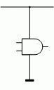
AND

out = A.B
| A | B | out |
| L | L | L |
| L | H | L |
| H | L | L |
| H | H | H |
OR

out = A + B
| A | B | out |
| L | L | L |
| L | H | H |
| H | L | H |
| H | H | H |
NOT

out =
| A | out |
| L | H |
| H | L |
Three-input gates
Three input gates do exist, they are basically two 2-input gates chained together.
NAND

out =
| A | B | out |
| L | L | H |
| L | H | H |
| H | L | H |
| H | H | L |
NOR

out = (this is not as the same as out= + )
| A | B | out |
| L | L | H |
| L | H | L |
| H | L | L |
| H | H | L |
XOR

out = B + A
| A | B | out |
| L | L | L |
| L | H | H |
| H | L | H |
| H | H | L |
Drawing Conventions
Normally, inputs are on the top and left of a piece of paper, and outputs are on the bottom and right.
These wires are unconnected.

These wires are connected
A combinatorial circuit is one whose outputs are entirely dependent on the current state of the inputs. All gates also act as buffers.
Dual in-line packages
These hold many types of gate and are connected via pins on either side. There are also 2 special pins, Vcc and GND, which provide the power for the chip. Plastic DIPs are low heat, but cheap. Ceramic DIPs are more expensive but can be opened under heat. They are also more durable.
Boolean Algebraic Manipulation
Logical Operations on Constants
NOT
= 0
0 =
AND
0.0 = 0
0.1 = 0
1.0 = 0
1.1 = 1
OR
0 + 0 = 0
0 + 1 = 1
1 + 0 = 1
1 + 1 = 1
Logical Operations on Variables
AND
A.0 = 0
A.1 = A
OR
A + 0 = A
A + 1 = 1
NOT
A. = 0
A + = 1
All TTLs float high by default.
Commutation
A + B = B + A
A.B = B.A
Association
A + B + C = A + (B + C) = (A + B) + C
A.B.C = A.(B.C) = (A.B).C
de Morgan's Theorem
= .
= +
Some Logical Manipulation
A.(B + C)
= A.B + A.C
(A + B).(C + D)
= A.C + B.C + B.D + A.D
A.B + A.
= A.(B + )
= A
A.(A + B)
= A + A.B
= A.(1 + B)
= A
XOR
C = .B + A.
De Morgan's Law
= +
Terminology
Product Term
A single variable or logical product of several variables. E.g., A, , .B.. This is basically the AND function. Note that is not a product term.
Sum Term
Sum term is the single variable or the logical sum of several variables. The variables may be in true, or complemented, form. E.g., + + C, etc... This is the OR function. Note that here also, is not a sum term.
Sum-of-products
This is product terms added together., e.g., A.B.C + .. + .Q. Note that ..C + is not a valid sum-of-products form.
Product-of-sums
This is the sum of several terms multiplied together, e.g., ( + B + C).(X + + J). Note that (A + + C). is not in product of sums form.
Canonical Forms
The first canonical form
If each variable is in the true of complimentary form and it appears in each term of the sub-products, then it is known as the canonical sum-of-products and each term is a minterm.
The second canonical form
This similar to the first canonical form, but each variable in a product-of-sums form and each term becomes a maxterm.
Minterm
A minterm is a product term which contains each variable in complimentary form. When used in the canonical sum-of-products, the minterm represent an input condition that causes the output to be 1.
Maxterm
A sum term which contains each variable in complimentary form. When used in the canonical product-of-sums the maxterm represents an input condition which causes the function to be 0.
Karnaugh Map
This is based on boolean algebra and is another method of minimisation.
| C\AB | 00 | 01 | 11 | 10 |
| 0 | 0 | 0 | 0 | 0 |
| 1 | 1 | 0 | 1 | 0 |
The order of bits on the top row is important. Only one bit can change between columns.
This is essentially a re-arranged truth table. Variables which appear together horizontally or vertically are logically adjacent.
If there are 2n maxterms, n is the number of rows that can be looped. The member of grouped minterms must be a power of 2.
- Make loops as big as possible
- Choose fewest loops possible
- Include all minterms
2n minterms are logically adjacent if there are n bits changed.
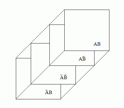
Five and six variable karnaugh maps can occur - these are represented in 3 dimensions.
E
| CD\AB | 00 | 01 | 11 | 10 |
| 00 | 1 | 1 | ||
| 01 | ||||
| 11 | ||||
| 10 | 1 | 1 |
| CD\AB | 00 | 01 | 11 | 10 |
| 00 | 1 | 1 | ||
| 01 | ||||
| 11 | ||||
| 10 | 1 | 1 | 1 |
E is on top of .
The same applies to a six-variable Karnaugh Map, which looks like this:
Maxterms can be looped up in a similar way to minterms, but are inverted.
Prime Implicants
These are the biggest adjacent terms which can be looped together. Single isolated implicants are also prime implicants.
Essential Prime Implicants
This is a prime implicant that contains a minterm not included in any other prime implicants. Isolated minterms are also essential prime implicants. An essential prime implicant must be included in the final expression.
Quine-McCluskey Minimisation
- Find all logically adjacent minterms to produce implicants - Tabulate all the minterms from the expressions and re-order them so that all the minterms without any 1's are together, the minterms with one 1 are together, etc. Then you need to write down pairs of logically adjacent minterms, these will give you the implicants. Replace the bits that make them logically adjacent with '-'
- Find all logically adjacent implicants to produce prime implicants. Repeat for all possible prime implicants - Find all logically adjacent implicants from the last step using the same process. Repeat until you have all adjacancies.
- Use a prime implicant table to determine essential prime implicants - From the previous step, any implicants that can not be reduced any further are prime.
- Select the minimum number of additional prime implicants to produce minimum expression - Plot a table of the prime implicants against the original minterms. Columns that only have one tick are essential.
- Choose best expression based on implementation issues
Quine-McCluskey is algorithmic. It is tedious and error prone when done by hand. However, it can be automated, and is guaranteed to find the set of minimal solutions. It works for maxterms as well as minterms.
Hardware Realisation
IC realisation requires minimising the number of gates. PCB realisation involves minimising the number of packages (therefore minimising the number of gates and gate types).
- OR-AND realisations, this is a minimised sum-of-products
- AND-OR realisations, this is a minimised product-of-sums.
- All NAND realisations. In an AND-OR realisation, replace all gates with NAND gates, then any input that goes directly to the second stage of gates (OR) needs to be inverted (which can be done using NAND gates).
- All NOR realisations. Replace all gates in an OR-AND realisation with NOR gates, and any input that goes directly to the stage of gates (AND) needs to be inverted. This can be done using a NOR gate.
In negative logic, an AND gate is an OR gate and an OR is an AND. When a NAND gate has positive logic inputs and negative logic outputs, it behaves like an AND. Similarly, is an OR gate has negative logic on inputs and positive logic on outputs, it behaves like an OR.
Map-Factoring (Inhibiting Functions)
This can be used when you nearly have a minterm, but there is one maxterm blocking it. If you realise a design assuming that the maxterm is indeed a minterm (and you then have a prime implicant) you can then add in an inhibiting function which stops the circuit being true unless the maxterm is false, making your assumption work as intended.
However, this increases gate delay, but does tend to lead to fewer gates or packages being used. It can also make it less obvious what a design is for.
Designing multiple-output circuits
You need to treat each circuit as if it were being generated by an independent circuit and look for common terms.
Don't Cares
Don't cares are input conditions that will never occur under normal operations and are marked as output X. You can treat a don't care as either a max-term or a min-term, whichever is more convenient for you. So, for example, you can loop a don't care with minterms or maxterms to create a more minimised expression. Don't cares by themselves are not looped however.
You need to take care, however, incase a don't care term does occur (for example during the initialisation of flip-flops, etc).
Design Considerations
Which hardware implementation to use? PCB, IC, PLD? Which device technology? TTL, CMOS transistors, ECL? Hardware environment? Temperature, radiation, pressure, vibrations, etc...
You need to minimise gates and packages, the gate layers (circuit delay), the number of interconnects between gates and between packages, maintenance costs, power consumption, weight, design costs, production costs, hazardous behaviour.
Design Steps
Check each stem!
- Obtain requirements - an imprecise statement of objectives
- Map requirements into a formal specification - truth table, etc
- Design the circuit - use minimisation
- Realise the circuit - consider any further minimisation
- Analyse the circuit - either by hand or on computer. Allow for production and environmental consideration.
- Prototype the circuit - check it on the lab under full range of conditions
- Test
Electrical Considerations
| Logic Families | Standard spec (e.g.,) | Military spec (e.g.,) |
| Old Standard | SN7400 | SN5400 |
| High Speed | SN74H00 | SN54H00 |
| Low Power | SN74L00 | SN54L00 |
| Schottky | SN74S00 | SN54S00 |
| Low Power Schottky | SN74LS00 | SN54LS00 |
| Advanced Schottky | SN74AS00 | SN54AS00 |
| Advanced Low Power Schottky | SN74ALS00 | SN54ALS00 |
Temperature ranges: Standard: 0 °C - 70 °C; Military -55 °C - 125 °C
Power Supply
Gates are supplied by power from a power supply via a power rail known as Vcc and ground. This power rail is implied and not actually show on circuit diagrams. In a dual-inline package, powering the package automatically powers all the gates.
Normally, the power supply is 5 V. For standard specification gates, the allowed variances are ±0.25 V and for military this is ±0.5 V. There is also an absolute voltage rating, above which the gate burns out. This is approximately 7 V.
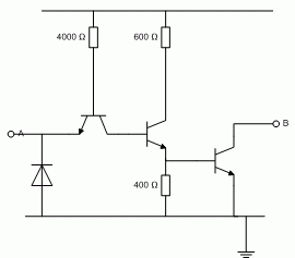
Totem Pole Output
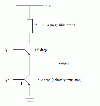
Output is high when Q1 is on and Q2 is off, inversely, output is low when Q1 is off and Q2 is on. During transitions, Q1 and Q2 both conduct, but current is limited by R1, this causes a "spike" to be seen on the supply rail and is known as electrical noise. The spike is caused by the sudden increase and then decrease in current required by the gate. Capacitors are evenly spread around a PCB according to some in-house rule of thumb. These "decoupling" capacitors are connected between supply rail and earth, supplying instantaneous current which the transistors need.
Fan-out
When the interconnecting node is low, current flows out of the second gate into the first one. The inverse happens when the interconnect is high.
In a data book, the following notations are used to signify currents:
- IOL - output when low
- IOH - output when high
- IIL - input when low
- IIH - input when high
Unused Inputs
NAND and NOR gates can be used as inverters. 4-input gates can be used by 2 variables only, etc... However, TTL inputs float high and CMOS floats low. For a TTL 4-input AND: ABC1 = ABC, but for a 4-input OR: A + B + C + 1 = 1, which is a tautology.
Unused inputs are susceptible to electrical noise and may slow down gate operation.
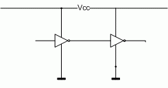
This is two different ways to make a 3-input gate work with two inputs (generating logic 0). The bottom method is preferred.
To generate logic 1, you can do something like this:
The bottom circuit can only be used with low-power Schottky, however. For other devices, you can tie them to the Vcc rail using a 1k Ω resistor.
TTL Voltage Levels
| Output | Input | |
| Logic 1 | 2.4-5.0 V | 2.0-5.0 V |
| Logic 0 | 0.0-0.4 V | 0.0-0.8 V |
Levels of Integration
SSI - small scale integration. 1 - 20 gates, up to 100 transistors, few gates and flip flops.
MSI - medium scale integration. 20 - 200 gates, functional building blocks.
LSI - large scale integration. 200 - 200,000 gates, PLDs and early microprocessors.
VLSI - very large scale integration. 500,000+ gates, 32-bit microprocessors, etc...
Propagation Delay
The propagation delay of a gate is the time it takes for the gate output to change in response to a change on its input. High-to-low delays may differ from low-high-delays.
tPHL is the time between specified reference points on the input and output voltage waveforms with the output changing from the defined high level to the defined low level.
tPLH is time between specified reference points on the input and output voltage waveforms with the output changing from the defined low level to the defined high level.
A static hazard is where there's a change from minterm to minterm (static-1) or maxterm to maxterm (static-0) and a "blip" occurs. A dynamic hazard is where there's a hazard in a change between max- and min-terms.
Buffers help mask propagation delays and can decrease hazards. This, however, isn't the best solution to hazards. Waveform analysis is a better indicator for predicting hazards, but it may not be accurate in reality.
System Organisation
These are dedicated buses.
A bus is a set of wires designed to transfer all bits of a word from a source to a destination.
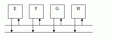
This is a shared bus.
Multibus (IEEE 796)
This standard defines a bus standard. There are 86 wires (16 bit bi-directional data bus, 24 bit address bus, 26 bit control bus (used for data-transfer commands, handshaking, etc) and a 20 bit power and ground line bus (8 GND, 8 +5 V, 2 +12 V, 2 -12 V)).
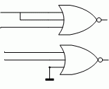
Open Collector Devices
These type of devices can accept voltages of ±15 V on the Vcc rail, and can therefore sink higher voltages. They are typically indicated by a star over the end of the gate. Because of this, you can do things like this:
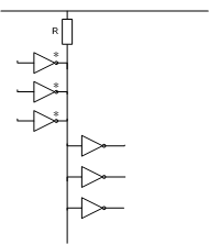
The value of R is calculated according to a formula specified by the manufacturer. The value must be re-calculated every time an input or output is added or removed.
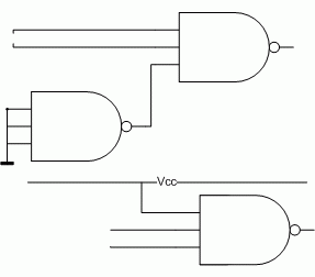
Wired-AND Gate
You can also do things like this to emulate AND gates:
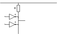
Which, by inspection, gives us an AND gate.
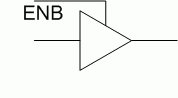
Tristate Devices
Tristate devices have 3 output states
- TTL logic 1 state
- TTL logic 0 state
- A high-impedance state
A tristate device can sink and drive large currents than TTL.
Bus Driver/Receiver
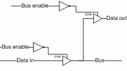
Of all the gates connected to a bus wire, only one should drive at once. All gates can be in a high impendence state, however.
Representation

This is a bidirectional bus

This is a unidirectional bus.
The number represents the bus width.
Signals takes a finite time to propagate and are therefore comparable to gate delay.
Characteristic Impedance
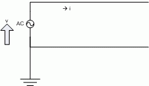
Z0 = v / i
| Z0 | |
| PCB tracks | 50 - 150 Ω |
| Twisted pair | 100 - 120 Ω |
| Coaxial cable | 50 - 75 Ω |
Multiplexing and Demultiplexing
A multiplexer switches from various inputs to an output, e.g., a mechanical one may be an input selector on a hi-fi amplifier. An electrical multiplexer: offers one logic load, have normal fan out, and have a strobe to enable/disable the mux (multiplexer).
A demultiplexer does the opposite - it puts an input onto the addressed output.
Programmable Logic Devices
PLDs have an inverting stage, an ANDing stage and an ORing stage. They have multiple I/Os and they realise sum-of-product expressions.
A programmer is a device to which an unprogrammed PLD is plugged. Using a programmer keyboard and a schematic of the device, internal connections can be located and blown away. Traditionally the method for doing this is:
- Create boolean equations
- Enter them into computer program
- Compile them into JEDEC form
- Programmer uses JEDEC file to program the PLD.
PROMs are general purpose decoders leading to an ORing stage. Only the ORing stage is programmable. PROMs are available in different varieties, such as:
- ROMs are programmed by the manufacturer, and are only cost-effective if manufactured in large quantities.
- PROMs are developed in a lab. Once the fuses are blown, they can't be reinstated. They are programmed by electrical pulses up the output.
- EPROMs, this are like PROMs, but UV light resets the fuses.
- EEPROMs, like EPROM, but electrical pulses are used to reinstate the fuses, not UV light.
For PLDs, instead of a conventional notation, crosses are put where wires intersect to indicate fuses being intact.
Programmable Gate Array
Inverters lead to NAND gates which lead to XOR gates. The XOR inverts. NAND gates and output polarity are programmable. If the polarity of the XOR gate is intact, the NAND gate is shown, otherwise the other input is set to logical 1 and inverted.
Programmable Array Logic
This is a programmable AND array, but a fixed OR array. In PALs, every output is not programmable with every possible input combination, however they are low cost and easily programmed. If you have any unused AND gates in the array, all fuses must be intact, which sets the output to 0 which doesn't interfere with the OR.
Some PALs have tristate buffers for bus driving (the tristate selects whether the PAL is an driving or receiving), hence the PAL can be used for inputs and outputs.
Programmable Logic Array
This has a programmable AND array and OR array.
PLDs have extra security to allow the device to be checked and allows the fuse arrays to be read. Some PLDs have security fuses to stop the devices being read.
IDD is continued straight through into DAD.